SLVSC25B July 2013 – June 2017 TPS61197
PRODUCTION DATA.
- 1 Features
- 2 Applications
- 3 Description
- 4 Revision History
- 5 Pin Configuration and Functions
- 6 Specifications
-
7 Detailed Description
- 7.1 Overview
- 7.2 Functional Block Diagram
- 7.3 Feature Description
- 7.4
Device Functional Modes
- 7.4.1
Protections
- 7.4.1.1 Switch Current Limit Protection Using the ISNS Pin
- 7.4.1.2 LED Open Protection
- 7.4.1.3 Schottky Diode Open Protection
- 7.4.1.4 Schottky Diode Short Protection
- 7.4.1.5 IFB Overvoltage Protection
- 7.4.1.6 Output Overvoltage Protection Using the OVP Pin
- 7.4.1.7 IFB Short-to-Ground Protection
- 7.4.1.8 Thermal Shutdown
- 7.4.1
Protections
- 8 Application and Implementation
- 9 Power Supply Recommendations
- 10Layout
- 11Device and Documentation Support
- 12Mechanical, Packaging, and Orderable Information
Package Options
Mechanical Data (Package|Pins)
- D|16
Thermal pad, mechanical data (Package|Pins)
- D|16
Orderable Information
1 Features
- 8-V to 30-V Input Voltage
- 50-kHz to 800-kHz Programmable Switching Frequency
- Adaptive Boost Output to White-LED Voltage
- High-Precision PWM Dimming Resolution up to 5000:1
- Programmable Overvoltage Protection Threshold at Output
- Programmable Undervoltage Threshold at Input with Adjustable Hysteresis
- Adjustable Soft-Start Time Independent of Dimming Duty Cycle
- Built-in LED Open and IFB Short Protections
- Built-in Schottky Diode Open/Short Protection
- Thermal Shutdown
2 Applications
- LCD TV Backlight
- Large LCD TV Displays
- Monitors
3 Description
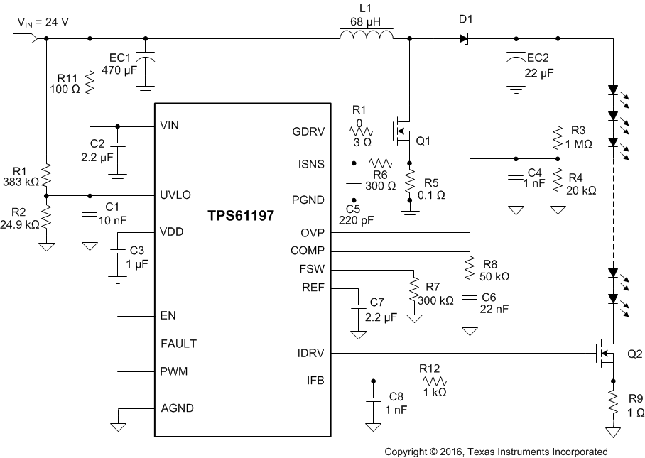
The TPS61197 provides highly integrated solutions for LCD TV backlighting. This device is a current-mode boost controller driving one WLED string with multiple LEDs in series. The TPS61197 adjusts the output voltage of the boost controller automatically to provide only the minimum voltage required by the LED string to generate the setting LED current, thereby optimizing the efficiency of the driver.
The device supports direct PWM brightness dimming method. During the pulse-width modulation (PWM) dimming, the white LED current is turned on and off at the duty cycle and frequency, which are determined by an external PWM signal. The PWM dimming frequency ranges from 90 Hz to 22 kHz.
The TPS61197 integrates overcurrent protection, output short-circuit protection, Schottky diode open and short protection, LED open protection, LED-string short protection, and overtemperature shutdown circuit. The device also provides programmable input undervoltage lockout (UVLO) threshold and output overvoltage protection (OVP) threshold. The device is available in a 16-pin SOIC package, which is ideal for a single-layer PCB board.
Device Information(1)
| PART NUMBER | PACKAGE | BODY SIZE (NOM) |
|---|---|---|
| TPS61197 | SOIC (16) | 17.90 mm × 7.50 mm |
- For all available packages, see the orderable addendum at the end of the data sheet.
Simplified Schematic
