SLVS776B January 2009 – November 2014 TPS61220 , TPS61221 , TPS61222
PRODUCTION DATA.
- 1 Features
- 2 Applications
- 3 Description
- 4 Simplified Schematic
- 5 Revision History
- 6 Pin Configuration and Functions
- 7 Specifications
- 8 Parameter Measurement Information
- 9 Detailed Description
- 10Applications and Implementation
- 11Power Supply Recommendations
- 12Layout
- 13Device and Documentation Support
- 14Mechanical, Packaging, and Orderable Information
Package Options
Mechanical Data (Package|Pins)
- DCK|6
Thermal pad, mechanical data (Package|Pins)
- DCK|6
Orderable Information
7 Specifications
7.1 Absolute Maximum Ratings
over operating free-air temperature range (unless otherwise noted)(1)| TPS6122x | UNIT | ||
|---|---|---|---|
| VIN | Input voltage on VIN, L, VOUT, EN, FB | –0.3 to 7.5 | V |
| TJ | Operating junction temperature | –40 to 150 | °C |
(1) Stresses beyond those listed under Absolute Maximum Ratings may cause permanent damage to the device. These are stress ratings only, and functional operation of the device at these or any other conditions beyond those indicated under Recommended Operating Conditions is not implied. Exposure to absolute-maximum-rated conditions for extended periods may affect device reliability.
7.2 Handling Ratings
| MIN | MAX | UNIT | |||
|---|---|---|---|---|---|
| Tstg | Storage temperature range | –65 | 150 | °C | |
| V(ESD) | Electrostatic discharge | Human body model (HBM), per ANSI/ESDA/JEDEC JS-001, all pins(1) | –2 | 2 | kV |
| Charged device model (CDM), per JEDEC specification JESD22-C101, all pins(2) | –1.5 | 1.5 | kV | ||
(1) JEDEC document JEP155 states that 500V HBM rating allows safe manufacturing with a standard ESD control process.
(2) JEDEC document JEP157 states that 250V CDM rating allows safe manufacturing with a standard ESD control process.
7.3 Recommended Operating Conditions
| MIN | NOM | MAX | UNIT | ||
|---|---|---|---|---|---|
| VIN | Supply voltage at VIN | 0.7 | 5.5 | V | |
| TJ | Operating virtual junction temperature | –40 | 125 | °C | |
7.4 Thermal Information
| THERMAL METRIC(1) | TPS6122x | UNIT | |
|---|---|---|---|
| DCK | |||
| 6 PINS | |||
| RθJA | Junction-to-ambient thermal resistance | 231.2 | °C/W |
| RθJCtop | Junction-to-case (top) thermal resistance | 61.8 | |
| RθJB | Junction-to-board thermal resistance | 78.8 | |
| ψJT | Junction-to-top characterization parameter | 2.2 | |
| ψJB | Junction-to-board characterization parameter | 78.0 | |
| RθJCbot | Junction-to-case (bottom) thermal resistance | n/a | |
(1) For more information about traditional and new thermal metrics, see the IC Package Thermal Metrics application report, SPRA953.
7.5 Electrical Characteristics
over recommended free-air temperature range and over recommended input voltage range (typical at an ambient temperature range of 25°C) (unless otherwise noted)| PARAMETER | TEST CONDITIONS | MIN | TYP | MAX | UNIT | ||
|---|---|---|---|---|---|---|---|
| DC/DC STAGE | |||||||
| VIN | Input voltage | 0.7 | 5.5 | V | |||
| VIN | Minimum input voltage at startup | RLoad ≥ 150 Ω | 0.7 | V | |||
| VOUT | TPS61220 output voltage | VIN < VOUT | 1.8 | 6.0 | V | ||
| VFB | TPS61220 feedback voltage | 483 | 500 | 513 | mV | ||
| VOUT | TPS61221 output voltage (3.3 V) | VIN < VOUT | 3.20 | 3.30 | 3.41 | V | |
| VOUT | TPS61222 output voltage (5 V) | VIN < VOUT | 4.82 | 5.00 | 5.13 | V | |
| ILH | Inductor current ripple | 200 | mA | ||||
| ISW | switch current limit | VOUT = 3.3 V, VIN = 1.2 V, TA = 25°C | 240 | 400 | mA | ||
| VOUT = 3.3 V | 200 | 400 | mA | ||||
| RDSon_HSD | Rectifying switch on resistance | VOUT = 3.3 V | 1000 | mΩ | |||
| VOUT = 5.0 V | 700 | mΩ | |||||
| RDSon_LSD | Main switch on resistance | VOUT = 3.3 V | 600 | mΩ | |||
| VOUT = 5.0 V | 550 | mΩ | |||||
| Line regulation | VIN < VOUT | 0.5% | |||||
| Load regulation | VIN < VOUT | 0.5% | |||||
| IQ | Quiescent current | VIN | IO = 0 mA, VEN = VIN = 1.2 V, VOUT = 3.3 V |
0.5 | 0.9 | μA | |
| VOUT | 5 | 7.5 | μA | ||||
| ISD | Shutdown current | VIN | VEN = 0 V, VIN = 1.2 V, VOUT ≥ VIN | 0.2 | 0.5 | μA | |
| ILKG_VOUT | Leakage current into VOUT | VEN = 0 V, VIN = 1.2 V, VOUT = 3.3 V | 1 | μA | |||
| ILKG_L | Leakage current into L | VEN = 0 V, VIN = 1.2 V, VL = 1.2 V, VOUT ≥ VIN | 0.01 | 0.2 | μA | ||
| IFB | TPS61220 Feedback input current | VFB = 0.5 V | 0.01 | μA | |||
| IEN | EN input current | Clamped on GND or VIN (VIN < 1.5 V) | 0.005 | 0.1 | μA | ||
| CONTROL STAGE | |||||||
| VIL | EN input low voltage | VIN ≤ 1.5 V | 0.2 × VIN | V | |||
| VIH | EN input high voltage | VIN ≤ 1.5 V | 0.8 × VIN | V | |||
| VIL | EN input low voltage | 5 V > VIN > 1.5 V | 0.4 | V | |||
| VIH | EN input high voltage | 5 V > VIN > 1.5 V | 1.2 | V | |||
| VUVLO | Undervoltage lockout threshold for turn off | VIN decreasing | 0.5 | 0.7 | V | ||
| Overvoltage protection threshold | 6.0 | 7.5 | V | ||||
| Overtemperature protection | 140 | °C | |||||
| Overtemperature hysteresis | 20 | °C | |||||
7.6 Typical Characteristics
| TABLE OF GRAPHS | FIGURE | |
|---|---|---|
| Maximum Output Current | versus Input Voltage (TPS61220, TPS61221, TPS61222) | Figure 1 |
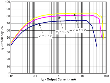
| Efficiency | versus Output Current, VOUT = 1.8 V, VIN = [0.7 V; 1.2 V; 1.5 V] (TPS61220) | Figure 2 |
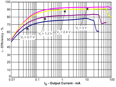
| versus Output Current, VIN = [0.7 V; 1.2 V; 2.4 V; 3 V] (TPS61221) | Figure 3 | |
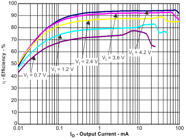
| versus Output Current, VIN = [0.7 V; 1.2 V; 2.4V; 3.6 V; 4.2 V] (TPS61222) | Figure 4 | |
| versus Input Voltage, VOUT = 1.8 V, IOUT = [100 µA; 1 mA; 10 mA; 50 mA] (TPS61220) | Figure 5 | |
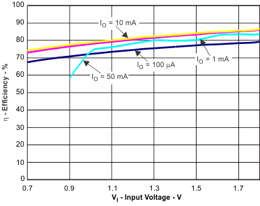
| versus Input Voltage, IOUT = [100 µA; 1 mA; 10 mA; 50 mA] (TPS61221) | Figure 6 | |
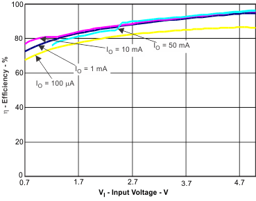
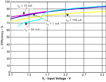
| versus Input Voltage, IOUT = [100 µA; 1 mA; 10 mA; 50 mA] (TPS61222) | Figure 7 | |
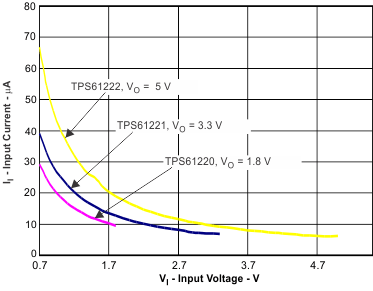
| Input Current | at No Output Load, Device Enabled (TPS61220, TPS61221, TPS61222) | Figure 8 |
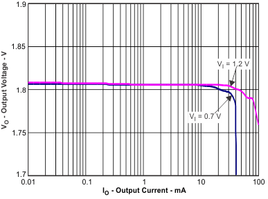
| Output Voltage | versus Output Current, VOUT = 1.8 V, VIN = [0.7 V; 1.2 V] (TPS61220 ) | Figure 9 |
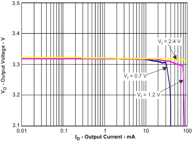
| versus Output Current, VIN = [0.7 V; 1.2 V; 2.4 V] (TPS61221) | Figure 10 | |
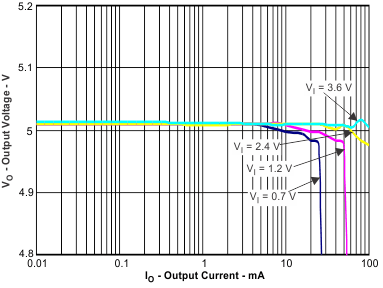
| versus Output Current, VIN = [0.7 V; 1.2 V; 2.4 V; 3.6 V] (TPS61222) | Figure 11 | |
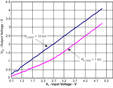
| versus Input Voltage, Device Disabled, RLOAD = [1 kΩ; 10 kΩ] (TPS6122x) | Figure 12 | |
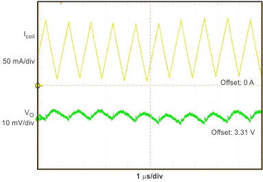
| Waveforms | Output Voltage Ripple, VIN = 0.8 V, VOUT = 1.8 V, IOUT = 20 mA (TPS61220) | Figure 13 |
| Output Voltage Ripple VIN = 1.8 V, IOUT = 50 mA (TPS61221) | Figure 14 | |
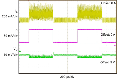
| Load Transient Response, VIN = 1.2 V, IOUT = 6 mA to 50 mA (TPS61221) | Figure 15 | |
| Load Transient Response, VIN = 2.4 V, IOUT = 14 mA to 126 mA (TPS61222) | Figure 16 | |
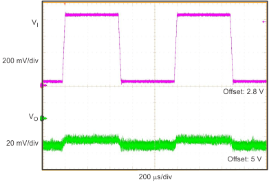
| Line Transient Response, VIN = 1.8 V to 2.4 V, RLOAD = 100 Ω (TPS61221) | Figure 17 | |
| Line Transient Response, VIN = 2.8 V to 3.6 V, RLOAD = 100 Ω (TPS61222) | Figure 18 | |
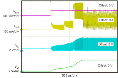
| Startup after Enable, VIN = 0.7 V, VOUT = 1.8 V, RLOAD = 150 Ω (TPS61220) | Figure 19 | |
| Startup after Enable, VIN = 0.7 V, RLOAD = 150 Ω, (TPS61222) | Figure 20 | |
| Continuous Current Operation, VIN = 1.2 V, VOUT = 1.8 V, IOUT = 50mA (TPS61220 ) | Figure 21 | |
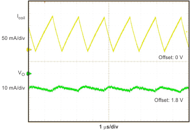
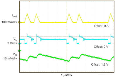
| Discontinuous Current Operation, VIN = 1.2 V, VOUT = 1.8 V, IOUT = 10mA (TPS61220) | Figure 22 | |
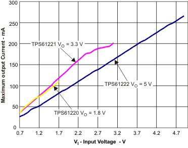
| VO = 3.3 V | ||
| VO = 1.8 V | ||
| VO = 5 V | ||
| VO = 1.8 V | ||
| VO = 5 V | ||
| VI = 0.8 V | VO = 1.8 V | IO = 20 mA |
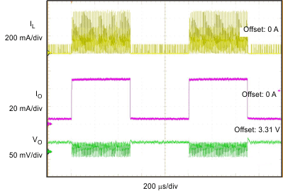
| VI = 1.2 V | IO = 6 mA to 50 mA | |
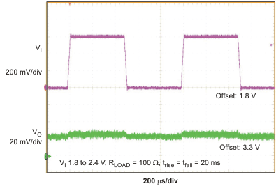
| VI = 2.4 V to 2.4 V | RLOAD = 100 Ω | trise = tfall = 20 ms |
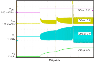
| VI = 0.7 V | VO = 1.8 V | RLOAD = 150 Ω |
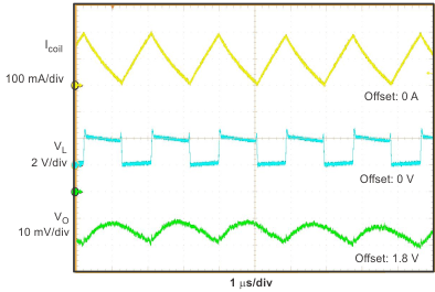
| VI = 1.2 V | VO = 1.8 V | IO = 50 mA |
| VO = 1.8 V | ||
| VO = 5 V | ||
| VO = 3.3 V | ||
| Device enabled | ||
| VO = 3.3 V | ||
| VEN = 0 V | ||
| VI = 1.8 V | VO = 3.3 V | IO = 50 mA |
| VI = 2.4 V | IO = 14 mA to 126 mA | |
| VI = 2.8 V to 3.6 V | RLOAD = 100 Ω | trise = tfall = 20 ms |
| VI = 0.7 V | VO = 3.3 V | RLOAD = 50 Ω |
| VI = 1.2 V | VO = 1.8 V | IO = 10 mA |