SLVSAQ2C January 2014 – October 2014 TPS61230 , TPS61232
UNLESS OTHERWISE NOTED, this document contains PRODUCTION DATA.
- 1 Features
- 2 Applications
- 3 Description
- 4 Revision History
- 5 Device Comparison Table
- 6 Pin Configuration and Functions
- 7 Specifications
- 8 Detailed Description
-
9 Applications and Implementation
- 9.1 Application Information
- 9.2
Typical Applications
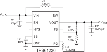
- 9.2.1 TPS61230 2.3-V to 5.5-V Input, 5-V Output Converter
- 9.2.2 TPS61230 2.3-V to 5.5-V Input, 3.5-V Output Converter
- 9.2.3 TPS61230 Application with Feed Forward Capacitor for Best Transient Response
- 10Power Supply Recommendations
- 11Layout
- 12Device and Documentation Support
- 13Mechanical, Packaging, and Orderable Information
Package Options
Mechanical Data (Package|Pins)
- DRC|10
Thermal pad, mechanical data (Package|Pins)
- DRC|10
Orderable Information
1 Features
- Input Voltage Range: 2.3 V to 5.5 V
- Output Voltage Range: 2.5 V to 5.5 V
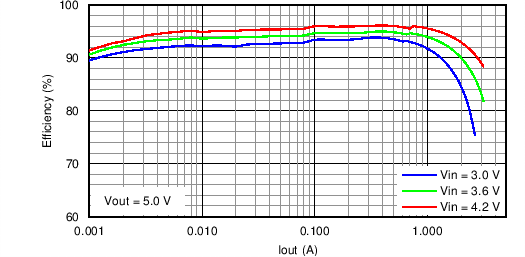
- Up to 96% Efficiency Synchronous Boost Converter
- 3.3-V to 5-V Power Conversion with 2.1-A Output Current
- Input Supply Voltage Supervisor with Adjustable Threshold/Hysteresis
- Power Save Mode for Light Load Efficiency
- Load Disconnect During Shutdown
- Output Over Voltage Protection
- Programmable Soft Start
- Power Good Output
- 2-MHz Switching Frequency
- Output Capacitor Discharge (TPS61231)
- 3 mm x 3 mm x 0.9 mm VSON Package
2 Applications
- Low Voltage Li-Ion Battery Powered Products
- USB Power Supply
- Tablet PCs
- Power Banks, Battery Backup Units
- Industrial Metering Equipments
3 Description
The TPS6123x device family is a high efficiency synchronous step up converter with compact solution size. It is optimized for products powered by a one-cell Li-Ion battery, or a regulated power rail of 3.3 V. The IC integrates a 5-A switch and is capable of delivering output currents up to 2.1 A at a 5-V output with a 3.3-V input supply. The device is based on a quasi-constant on-time valley current mode control scheme. The typical operating frequency is 2 MHz, which allows the use of small inductors and capacitors to achieve a small solution size. The TPS61230 and TPS61231 provide an adjustable output voltage via an external resistor divider, and the TPS61232 provides a fixed output voltage of 5 V.
During light loads, the TPS6123x automatically enters power save mode for maximum efficiency at lowest quiescent currents. In shutdown, the load is completely disconnected from the input, and the input current consumption is reduced to 1.5 µA typical. The device integrates a precise low power EN comparator. The EN threshold as well as the hysteresis of the enable comparator are adjustable with external resistors and support application specific system power up and down requirements. Other features like output over voltage protection, thermal shutdown protection, and a power good output are built-in.
The devices are available in a 3 mm x 3 mm x 0.9 mm VSON package.
Device Information(1)
| PART NUMBER | PACKAGE | BODY SIZE (NOM) |
|---|---|---|
| TPS61230 | VSON (10) | 3.00 mm x 3.00 mm |
| TPS61231(2) | ||
| TPS61232 |
- For all available packages, see the orderable addendum at the end of the datasheet.
- Preview product. Contact TI factory for more information
TPS61230 Typical Application
TPS61230 Typical Application Efficiency