SLVSCK4A September 2015 – May 2016 TPS61235P , TPS61236P
PRODUCTION DATA.
- 1 Features
- 2 Applications
- 3 Description
- 4 Revision History
- 5 Device Comparison Table
- 6 Pin Configuration and Functions
- 7 Specifications
-
8 Detailed Description
- 8.1 Overview
- 8.2 Functional Block Diagram
- 8.3
Feature Description
- 8.3.1 Boost Controller Operation
- 8.3.2 Soft Start
- 8.3.3 Enable and Disable
- 8.3.4 Constant Output Voltage and Constant Output Current Operations
- 8.3.5 Over Current Protection
- 8.3.6 Load Status Indication
- 8.3.7 Under voltage Lockout
- 8.3.8 Over Voltage Protection and Reverse Current Block
- 8.3.9 Short Circuit Protection
- 8.3.10 Thermal Shutdown
- 8.4 Device Functional Modes
-
9 Applications and Implementation
- 9.1 Application Information
- 9.2
Typical Applications
- 9.2.1
TPS61236P 3-V to 4.35-V Input, 5-V Output Voltage, 3-A Maximum Output Current
- 9.2.1.1 Design Requirements
- 9.2.1.2 Detailed Design Procedure
- 9.2.1.3 TPS61236P 5-V Output Application Curves
- 9.2.2 TPS61236P 2.3-V to 5-V Input, 5-V 2-A Output Converter
- 9.2.1
TPS61236P 3-V to 4.35-V Input, 5-V Output Voltage, 3-A Maximum Output Current
- 10Power Supply Recommendations
- 11Layout
- 12Device and Documentation Support
- 13Mechanical, Packaging, and Orderable Information
Package Options
Mechanical Data (Package|Pins)
- RWL|9
Thermal pad, mechanical data (Package|Pins)
Orderable Information
11 Layout
11.1 Layout Guidelines
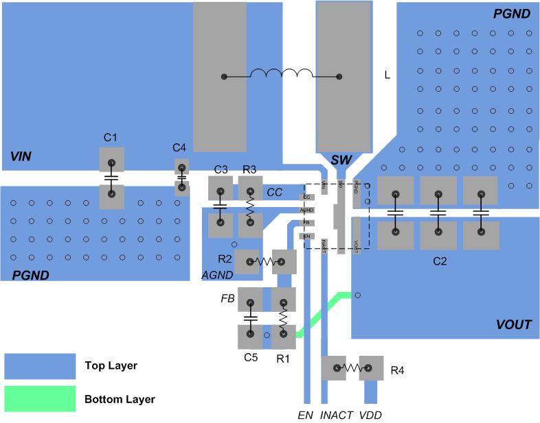
For all switching power supplies, layout is an important step in the design, especially at high peak currents and high switching frequencies. If the layout is not carefully done, the regulator could show stability problems as well as EMI problems. Therefore, use wide and short traces for the main current paths and the power ground tracks. The input capacitor, output capacitor, and the inductor should be placed as close as possible to the IC. Use a common ground node for power ground and a different one for control/analog ground to minimize the effects of ground noise. Connect these ground nodes near the ground pins of the IC. The most critical current path for all boost converters is from the switching FET, through the synchronous FET, the output capacitors, and back to the ground of the switching FET. Therefore, the output capacitors and their traces should be placed on the same board layer as the IC and as close as possible between the VOUT and PGND pins of the IC.
See Figure 39 for the recommended layout.
11.2 Layout Example
The bottom layer is a large GND plane connected by vias.
 Figure 39. Layout Recommendation
11.3 Thermal Considerations
The maximum IC junction temperature should be restricted to 125°C under normal operating conditions. Calculate the maximum allowable dissipation, PD(max), and keep the actual power dissipation less than or equal to PD(max). The maximum power dissipation limit is determined using:

Where:
TA is the maximum ambient temperature for the application.
RθJA is the junction-to-ambient thermal resistance given in the Thermal Information table.
The TPS6123x handles high power conversion so requires special attention to the power dissipation. The junction-to-ambient thermal resistance of a package in an application greatly depends on the PCB type and layout, and many system-dependent factors such as thermal coupling, airflow, added heat sinks and convection surfaces, and the presence of other heat-generating components also affect the power-dissipation limits.
Two common basic approaches to enhancing thermal performance are listed below.
- Increase the power dissipation capability of the PCB. It is necessary to have sufficient copper area as heat sinks. For DC voltage nodes like VIN, VOUT, and PGND, make the copper area as large as possible. Multiple vias are helpful in further reducing thermal stress. It is also a good practice to have thick copper layers in order to minimize the PCB conduction loss and thermal impedance.
- Introduce airflow in the system.
For more details on how to use the thermal parameters in the Thermal Information table, check the Thermal Characteristics Application Note (SZZA017) and the IC Package Thermal Metrics Application Note (SPRA953).