SLVSBD8A April 2014 – May 2014 TPS62095
PRODUCTION DATA.
- 1 Features
- 2 Applications
- 3 Description
- 4 Revision History
- 5 Pin Configuration and Functions
- 6 Specifications
- 7 Detailed Description
- 8 Application and Implementation
- 9 Power Supply Recommendations
- 10Layout
- 11Device and Documentation Support
- 12Mechanical, Packaging, and Orderable Information
Package Options
Mechanical Data (Package|Pins)
- RGT|16
Thermal pad, mechanical data (Package|Pins)
- RGT|16
Orderable Information
1 Features
- DCS-Control™ Topology
- Pin-to-Pin Compatible with TPS62090
- Supports 1.2mm Height Total Solution
- 95% Converter Efficiency
- 20µA Operating Quiescent Current
- 2.5V to 5.5V Input Voltage Range
- Power Save Mode
- Two Level Short Circuit Protection
- 100% Duty Cycle for Lowest Dropout
- Output Discharge Function
- Adjustable Soft Startup
- Output Voltage Tracking
- 0.8V to VIN Adjustable Output Voltage
- 3mm x 3mm 16-Pin VQFN Package
2 Applications
- Notebooks, Computers
- Solid State Drives
- Hard Disk Drives
- Processor Supply
- Battery Powered Applications
3 Description
The TPS62095 device is a high frequency synchronous step down converter optimized for small solution size, high efficiency and suitable for battery powered applications. To maximize efficiency, the converter operates in PWM mode with a nominal switching frequency of 1.4MHz and automatically enters Power Save Mode operation at light load currents. When used in distributed power supplies and point of load regulation, the device allows voltage tracking to other voltage rails and tolerates output capacitors up to 150µF and beyond. Using the DCS-Control™ topology, the device achieves excellent load transient performance and accurate output voltage regulation.
The output voltage startup ramp is controlled by the soft startup pin, which allows operation as either a standalone power supply or in tracking configurations. Power sequencing is also possible by configuring the EN and PG pins. In Power Save Mode, the device operates with typically 20µA quiescent current. Power Save Mode is entered automatically and seamlessly maintaining high efficiency over the entire load current range.
Device Information(1)
| PART NUMBER | PACKAGE | BODY SIZE (NOM) |
|---|---|---|
| TPS62095 | VQFN (16) | 3.00 mm × 3.00 mm |
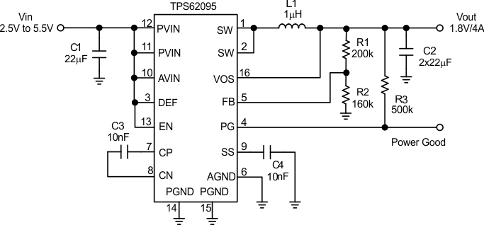
1.8V Output Application
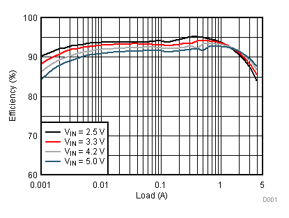
1.8V Output Application Efficiency