SLVS681F June 2006 – August 2014 TPS62400 , TPS62401 , TPS62402 , TPS62403 , TPS62404
PRODUCTION DATA.
- 1 Features
- 2 Applications
- 3 Description
- 4 Revision History
- 5 Device Options
- 6 Pin Configuration and Functions
- 7 Specifications
- 8 Detailed Description
-
9 Application and Implementation
- 9.1 Application Information
- 9.2
Typical Applications
- 9.2.1
TPS6240x, Dual Outputs Step Down Converter
- 9.2.1.1 Design Requirements
- 9.2.1.2
Detailed Design Procedure
- 9.2.1.2.1 Converter1 Adjustable Default Output Voltage Setting: TPS62400
- 9.2.1.2.2 Converter1 Fixed Default Output Voltage Setting (TPS62401, TPS62402, TPS62403, TPS62404).
- 9.2.1.2.3 Converter 2 Adjustable Default Output Voltage Setting TPS62400:
- 9.2.1.2.4 Converter 2 Fixed Default Output Voltage Setting
- 9.2.1.2.5 Output Filter Design (Inductor and Output Capacitor)
- 9.2.1.3 Application Curves
- 9.2.2 Various Output Voltages
- 9.2.3 Dynamic Voltage Scaling on Converter 1 by DEF_1 Pin
- 9.2.1
TPS6240x, Dual Outputs Step Down Converter
- 10Power Supply Recommendations
- 11Layout
- 12Device and Documentation Support
- 13Mechanical, Packaging, and Orderable Information
Package Options
Mechanical Data (Package|Pins)
- DRC|10
Thermal pad, mechanical data (Package|Pins)
- DRC|10
Orderable Information
11 Layout
11.1 Layout Guidelines
As for all switching power supplies, the layout is an important step in the design. Proper function of the device demands careful attention to PCB layout. Care must be taken in board layout to get the specified performance. If the layout is not carefully done, the regulator could show poor line and/or load regulation, stability issues as well as EMI problems. It is critical to provide a low-inductance, impedance ground path. Therefore, use wide and short traces for the main current paths as indicated in bold in Figure 48.
The input capacitor should be placed as close as possible to the IC pins VIN and GND, the inductor and output capacitor as close as possible to the pins SW1 and GND.
Connect the GND Pin of the device to the PowerPAD of the PCB and use this Pad as a star point. For each converter use a common Power GND node and a different node for the signal GND to minimize the effects of ground noise. Connect these ground nodes together to the PowerPAD (star point) underneath the IC. Keep the common path to the GND PIN, which returns the small signal components and the high current of the output capacitors, as short as possible to avoid ground noise. The output voltage sense lines (FB 1, DEF_1, ADJ2) should be connected right to the output capacitor and routed away from noisy components and traces (e.g., SW1 and SW2 lines). If the EasyScale™ interface is operated with high transmission rates, the MODE/DATA trace must be routed away from the ADJ2 line to avoid capacitive coupling into the ADJ2 pin. A GND guard ring between the MODE/DATA pin and ADJ2 pin avoids potential noise coupling.
11.2 Layout Example
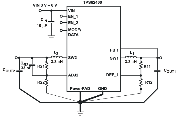 Figure 48. Layout Diagram
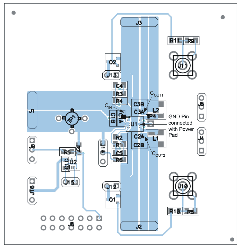 Figure 49. PCB Layout