SLVS681F June 2006 – August 2014 TPS62400 , TPS62401 , TPS62402 , TPS62403 , TPS62404
PRODUCTION DATA.
- 1 Features
- 2 Applications
- 3 Description
- 4 Revision History
- 5 Device Options
- 6 Pin Configuration and Functions
- 7 Specifications
- 8 Detailed Description
-
9 Application and Implementation
- 9.1 Application Information
- 9.2
Typical Applications
- 9.2.1
TPS6240x, Dual Outputs Step Down Converter
- 9.2.1.1 Design Requirements
- 9.2.1.2
Detailed Design Procedure
- 9.2.1.2.1 Converter1 Adjustable Default Output Voltage Setting: TPS62400
- 9.2.1.2.2 Converter1 Fixed Default Output Voltage Setting (TPS62401, TPS62402, TPS62403, TPS62404).
- 9.2.1.2.3 Converter 2 Adjustable Default Output Voltage Setting TPS62400:
- 9.2.1.2.4 Converter 2 Fixed Default Output Voltage Setting
- 9.2.1.2.5 Output Filter Design (Inductor and Output Capacitor)
- 9.2.1.3 Application Curves
- 9.2.2 Various Output Voltages
- 9.2.3 Dynamic Voltage Scaling on Converter 1 by DEF_1 Pin
- 9.2.1
TPS6240x, Dual Outputs Step Down Converter
- 10Power Supply Recommendations
- 11Layout
- 12Device and Documentation Support
- 13Mechanical, Packaging, and Orderable Information
Package Options
Mechanical Data (Package|Pins)
- DRC|10
Thermal pad, mechanical data (Package|Pins)
- DRC|10
Orderable Information
7 Specifications
7.1 Absolute Maximum Ratings
over operating free-air temperature range (unless otherwise noted)(1)| MIN | MAX | UNIT | |||
|---|---|---|---|---|---|
| Input voltage range on VIN(2) | –0.3 | 7 | V | ||
| Voltage range on EN, MODE/DATA, DEF_1 | –0.3 | VIN +0.3, ≤ 7 | V | ||
| current into MODE/DATA | ≤ 0.5 | mA | |||
| Voltage on SW1, SW2 | –0.3 | 7 | V | ||
| Voltage on ADJ2, FB1 | –0.3 | VIN +0.3, ≤ 7 | V | ||
| TJ(max) | Maximum operating junction temperature | 150 | °C | ||
| TA | Operating ambient temperature range | –40 | 85 | °C | |
(1) Stresses beyond those listed under absolute maximum ratings may cause permanent damage to the device. These are stress ratings only, and functional operation of the device at these or any other conditions beyond those indicated under recommended operating conditions is not implied. Exposure to absolute–maximum–rated conditions for extended periods may affect device reliability.
(2) All voltage values are with respect to network ground terminal.
7.2 Handling Ratings
| MIN | MAX | UNIT | |||
|---|---|---|---|---|---|
| Tstg | Storage temperature range | –65 | 150 | °C | |
| V(ESD) | Electrostatic discharge(3) | Human body model (HBM), per ANSI/ESDA/JEDEC JS-001, all pins(1) | 1 | kV | |
| Charged device model (CDM), per JEDEC specification JESD22-C101, all pins(2) | 0.5 | ||||
| Machine model | 200 | V | |||
(1) JEDEC document JEP155 states that 500-V HBM allows safe manufacturing with a standard ESD control process.
(2) JEDEC document JEP157 states that 250-V CDM allows safe manufacturing with a standard ESD control process.
(3) The human body model is a 100pF capacitor discharged through a 1.5kΩ resistor into each pin. The machine model is a 200pF capacitor discharged directly into each pin.
7.3 Recommended Operating Conditions
over operating free-air temperature range (unless otherwise noted)| MIN | NOM | MAX | UNIT | |||
|---|---|---|---|---|---|---|
| VIN | Supply voltage | 2.5 | 6 | V | ||
| VOUT | Output voltage range for adjustable voltage | 0.6 | VIN | V | ||
| TA | Operating ambient temperature | -40 | 85 | °C | ||
| TJ | Operating junction temperature | -40 | 125 | °C | ||
7.4 Thermal Information
| THERMAL METRIC(1) | TPS6240x | UNIT | |
|---|---|---|---|
| VSON | |||
| 10 PINS | |||
| RθJA | Junction-to-ambient thermal resistance | 45.9 | °C/W |
| RθJC(top) | Junction-to-case (top) thermal resistance | 64.3 | |
| RθJB | Junction-to-board thermal resistance | 20.4 | |
| ψJT | Junction-to-top characterization parameter | 1.3 | |
| ψJB | Junction-to-board characterization parameter | 20.6 | |
| RθJC(bot) | Junction-to-case (bottom) thermal resistance | 2.8 | |
(1) For more information about traditional and new thermal metrics, see the IC Package Thermal Metrics application report, SPRA953.
7.5 Electrical Characteristics
VIN = 3.6V, VOUT = 1.8V, EN = VIN, MODE = GND, L = 2.2μH, COUT = 20μF, TA = –40°C to 85°C typical values are atTA = 25°C (unless otherwise noted)
| PARAMETER | TEST CONDITIONS | MIN | TYP | MAX | UNIT | ||
|---|---|---|---|---|---|---|---|
| SUPPLY CURRENT | |||||||
| VIN | Input voltage range | 2.5 | 6.0 | V | |||
| IQ | Operating quiescent current | One converter, IOUT = 0mA. PFM mode enabled (Mode = 0) device not switching, EN1 = 1 OR EN2 = 1 |
19 | 29 | μA | ||
| Two converter, IOUT = 0mA. PFM mode enabled (Mode = 0) device not switching, EN1 = 1 AND EN2 = 1 |
32 | 48 | μA | ||||
| IOUT = 0mA, MODE/DATA = GND, for one converter, VOUT 1.575V(1) | 23 | μA | |||||
| IOUT = 0mA, MODE/DATA = VIN, for one converter, VOUT 1.575V (1) | 3.6 | mA | |||||
| ISD | Shutdown current | EN1, EN2 = GND, VIN = 3.6V(2) | 1.2 | 3 | μA | ||
| EN1, EN2 = GND, VIN ramped from 0V to 3.6V(3) | 0.1 | 1 | |||||
| VUVLO | Undervoltage lockout threshold | Falling | 1.5 | 2.35 | V | ||
| Rising | 2.4 | ||||||
| ENABLE EN1, EN2 | |||||||
| VIH | High-level input voltage range, EN1, EN2 | 1.2 | VIN | V | |||
| VIL | Low-level input voltage range, EN1, EN2 | 0 | 0.4 | V | |||
| IIN | Input bias current, EN1, EN2 | EN1, EN2 = GND or VIN | 0.05 | 1.0 | μA | ||
| DEF_1 INPUT | |||||||
| VDEF_1H | DEF_1 high level input voltage range | VOUT1 = fixed output voltage option | 0.9 | VIN | V | ||
| VDEF_1L | DEF_1 low level input voltage range | VOUT1 = fixed output voltage option | 0 | 0.4 | V | ||
| IIN | Input bias current DEF_1 | DEF_1 GND or VIN | 0.01 | 1.0 | μA | ||
| MODE/DATA | |||||||
| VIH | High-level input voltage range, MODE/DATA | 1.2 | VIN | V | |||
| VIL | Low-level input voltage range, MODE/DATA | 0 | 0.4 | V | |||
| IIN | Input bias current, MODE/DATA | MODE/DATA = GND or VIN | 0.01 | 1.0 | μA | ||
| VOH | Acknowledge output voltage high | Open drain, via external pullup resistor | VIN | V | |||
| VOL | Acknowledge output voltage low | Open drain, sink current 500μA | 0 | 0.4 | V | ||
| INTERFACE TIMING | |||||||
| tStart | Start time | 2 | μs | ||||
| tH_LB | High time low bit, logic 0 detection | Signal level on MODE/DATA pin is > 1.2V | 2 | 200 | μs | ||
| tL_LB | Low time low bit, logic 0 detection | Signal level on MODE/DATA pin < 0.4V | 2x tH_LB | 400 | μs | ||
| tL_HB | Low time high bit, logic 1 detection | Signal level on MODE/DATA pin < 0.4V | 2 | 200 | μs | ||
| tH_HB | High time high bit, logic 1 detection | Signal level on MODE/DATA pin is > 1.2V | 2x tL_HB | 400 | μs | ||
| TEOS | End of Stream | TEOS | 2 | μs | |||
| tACKN | Duration of acknowledge condition (MODE/DATE line pulled low by the device) | VIN 2.5V to 6V | 400 | 520 | μs | ||
| tvalACK | Acknowledge valid time | 2 | μs | ||||
| ttimeout | Timeout for entering power save mode | MODE/DATA Pin changes from high to low | 520 | μs | |||
| POWER SWITCH | |||||||
| RDS(ON) | P-Channel MOSFET on-resistance, Converter 1,2 | VIN = VGS = 3.6V | 280 | 620 | mΩ | ||
| ILK_PMOS | P-Channel leakage current | VDS = 6.0V | 1 | μA | |||
| RDS(ON) | N-Channel MOSFET on-resistance Converter 1,2 | VIN = VGS = 3.6V | 200 | 450 | mΩ | ||
| ILK_SW1/SW2 | Leakage current into SW1/SW2 pin | Includes N-Chanel leakage current, VIN = open, VSW = 6.0V, EN = GND(4) |
6 | 7.5 | μA | ||
| ILIMF | Forward Current Limit PMOS and NMOS | OUTPUT 1 | 2.5V ≤ VIN ≤ 6.0V | 0.68 | 0.8 | 0.92 | A |
| OUTPUT 2 | 0.85 | 1.0 | 1.15 | ||||
| TSD | Thermal shutdown | Increasing junction temperature | 150 | °C | |||
| Thermal shutdown hysteresis | Decreasing junction temperature | 20 | °C | ||||
| OSCILLATOR | |||||||
| fSW | Oscillator frequency | 2.5V ≤ VIN ≤ 6V | 2.0 | 2.25 | 2.5 | MHz | |
| OUTPUT | |||||||
| VOUT | Adjustable output voltage range | 0.6 | VIN | V | |||
| Vref | Reference voltage | 600 | mV | ||||
| VOUT (PFM) | DC output voltage accuracy adjustable and fixed output voltage(7) | Voltage positioning active, MODE/DATA = GND, device operating in PFM mode, VIN = 2.5V to 5.0V (5)(8) |
–1.5% | 1.01 VOUT | 2.5% | ||
| VOUT(PWM) | MODE/DATA = GND; device operating in PWM Mode, VIN = 2.5V to 6.0V(8) |
–1% | 0% | 1% | |||
| VIN = 2.5V to 6.0V, Mode/Data = VIN , Fixed PWM operation, 0mA < IOUT1 < 400mA ; 0mA < IOUT2 < 600mA(6) |
–1% | 0% | 1% | ||||
| DC output voltage load regulation | PWM operation mode | 0.5 | %/A | ||||
| tStart up | Start-up time | Activation time to start switching(9) | 170 | μs | |||
| tRamp | VOUT Ramp UP time | Time to ramp from 5% to 95% of VOUT | 750 | μs | |||
(1) Device is switching with no load on the output, L = 3.3μH, value includes losses of the coil
(2) These values are valid after the device has been already enabled one time (EN1 or EN2 = high) and supply voltage VIN has not powered down.
(3) These values are valid when the device is disabled (EN1 and EN2 low) and supply voltage VIN is powered up. The values remain valid until the device has been enabled first time (EN1 or EN2 = high). After first enable, Note 3 becomes valid.
(4) On pins SW1 and SW2 an internal resistor of 1MΩ is connected to GND.
(5) Configuration L typ 2.2μH, COUT typ 20μF, see parameter measurement information, the output voltage ripple in PFM mode depends on the effective capacitance of the output capacitor, larger output capacitors lead to tighter output voltage tolerance.
(6) For VOUT > 2V, VIN min = VOUT +0.5V
(7) Output voltage specification does not include tolerance of external voltage programming resistors
(8) In Power Save Mode, PWM operation is typically entered at IPSM = VIN/32Ω.
(9) This time is valid if one converter turns from shutdown mode (EN2 = 0) to active mode (EN2 = 1) AND the other converter is already enabled (e.g., EN1 = 1). In case both converters are turned from shutdown mode (EN1 and EN2 = low) to active mode (EN1 and/or EN2=1) a value of typ 80 μs for ramp up of internal circuits needs to be added. After tStart the converter starts switching and ramps VOUT.
7.6 Typical Characteristics
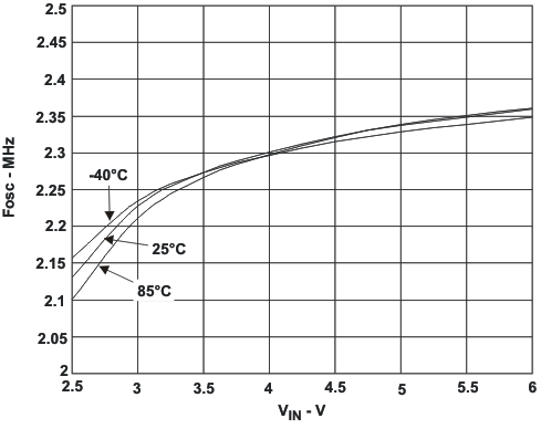
A.
Figure 1. FOSC vs VIN
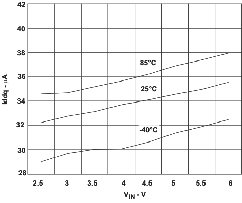
A.
Figure 3. Iq For Both Converters, Not Switching
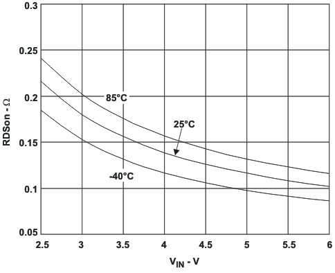
A.
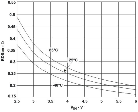
Figure 5. RDSON NMOS vs VIN
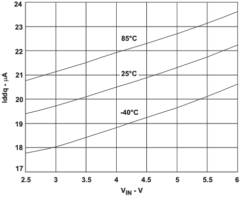
A.
Figure 2. Iq For One Converter, Not Switching
A.
Figure 4. RDSON PMOS vs VIN