SLVS952G April 2010 – January 2017 TPS62671 , TPS62672 , TPS62674 , TPS62675 , TPS626751 , TPS626765 , TPS62679
PRODUCTION DATA.
- 1 Features
- 2 Applications
- 3 Description
- 4 Simplified Schematic
- 5 Revision History
- 6 Device Comparison Table
- 7 Pin Configuration and Functions
- 8 Specifications
- 9 Parameter Measurement Information
- 10Detailed Description
- 11Application and Implementation
- 12Power Supply Recommendations
- 13Layout
- 14Device and Documentation Support
- 15Mechanical, Packaging, and Orderable Information
Package Options
Mechanical Data (Package|Pins)
- YFD|6
Thermal pad, mechanical data (Package|Pins)
Orderable Information
1 Features
- 92% Efficiency at 6MHz Operation
- 17μA Quiescent Current
- Wide VIN Range From 2.3V to 4.8V
- 6MHz Regulated Frequency Operation
- Spread Spectrum, PWM Frequency Dithering
- Best in Class Load and Line Transient
- ±2% Total DC Voltage Accuracy
- Low Ripple Light-Load PFM Mode
- ≥35dB VIN PSRR (1kHz to 10kHz)
- Simple Logic Enable Inputs
- Supports External Clock Presence Detect Enable Input
- Three Surface-Mount External Components Required (One 0603 MLCC Inductor, Two 0402 Ceramic Capacitors)
- Complete Sub 0.33-mm Component Profile Solution
- Total Solution Size <10 mm2
- Available in a 6-Pin NanoFree™ (CSP)
Ultra-Thin Packaging, 0.4 mm Max. Height
2 Applications
- Cell Phones, Smart-Phones
- CMOS Camera Module, Optical Data Module
- Digital TV, WLAN, GPS and Bluetooth™ Applications
- Embedded Power Supply
3 Description
The TPS6267x devices are high-frequency synchronous step-down dc-dc converters optimized for small battery-powered applications. Intended for low-power applications, the TPS6267x supports up to 650-mA load current and allows the use of low cost chip inductor and capacitors.
With a wide input voltage range of 2.3V to 4.8V, the device supports applications powered by Li-Ion batteries with extended voltage range. Different fixed voltage output versions are available from 1.05V to 2.1V. The TPS6267x operates at a regulated 6-MHz switching frequency and enters the power-save mode operation at light load currents to maintain high efficiency over the entire load current range.
The PFM mode extends the battery life by reducing the quiescent current to 17μA (typ) during light load operation. For noise-sensitive applications, the device has PWM spread spectrum capability providing a lower noise regulated output, as well as low noise at the input. These features, combined with high PSRR and AC load regulation performance, make this device suitable to replace a linear regulator to obtain better power conversion efficiency.
Device Information(1)
| PART NUMBER | PACKAGE | BODY SIZE (NOM) |
|---|---|---|
| TPS62671, TPS62672, TPS62674, TPS62675, TPS626751, TPS626765 | DSBGA (6) | 1.22mm x 0.85mm |
| TPS62679 | PicoStar (6) | 1.22mm x 0.85mm |
- For all available packages, see the orderable addendum at the end of the datasheet.
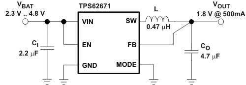
4 Simplified Schematic

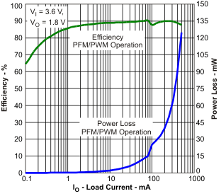
Efficiency vs Output Current
