SLVS952G April   2010  – January 2017 TPS62671 , TPS62672 , TPS62674 , TPS62675 , TPS626751 , TPS626765 , TPS62679

PRODUCTION DATA.  

  1. Features
  2. Applications
  3. Description
  4. Simplified Schematic
  5. Revision History
  6. Device Comparison Table
  7. Pin Configuration and Functions
  8. Specifications
    1. 8.1 Absolute Maximum Ratings
    2. 8.2 Handling Ratings
    3. 8.3 Recommended Operating Conditions
    4. 8.4 Thermal Information
    5. 8.5 Electrical Characteristics
    6. 8.6 Typical Characteristics
  9. Parameter Measurement Information
  10. 10Detailed Description
    1. 10.1 Overview
    2. 10.2 Functional Block Diagram
    3. 10.3 Feature Description
      1. 10.3.1 Switching Frequency
      2. 10.3.2 Power Save Mode
      3. 10.3.3 Mode Selection
      4. 10.3.4 Spread Spectrum, PWM Frequency Dithering
      5. 10.3.5 Short-Circuit Protection
      6. 10.3.6 Thermal Shutdown
    4. 10.4 Device Functional Modes
      1. 10.4.1 Soft Start
      2. 10.4.2 Enable
      3. 10.4.3 Active Output Discharge
      4. 10.4.4 Undervoltage Lockout
  11. 11Application and Implementation
    1. 11.1 Application Information
    2. 11.2 Typical Applications
      1. 11.2.1 TPS6267x Point-Of-Load Supply
        1. 11.2.1.1 Design Requirements
        2. 11.2.1.2 Detailed Design Procedure
          1. 11.2.1.2.1 Inductor Selection
          2. 11.2.1.2.2 Output Capacitor Selection
          3. 11.2.1.2.3 Input Capacitor Selection
          4. 11.2.1.2.4 Checking Loop Stability
        3. 11.2.1.3 Application Curves
      2. 11.2.2 1.26V CMOS Sensor Embedded Power Solution — Featuring Sub 0.4mm Profile
        1. 11.2.2.1 Design Requirements
        2. 11.2.2.2 Detailed Design Procedure
        3. 11.2.2.3 Application Curves
  12. 12Power Supply Recommendations
  13. 13Layout
    1. 13.1 Layout Guidelines
    2. 13.2 Layout Example
  14. 14Device and Documentation Support
    1. 14.1 Device Support
      1. 14.1.1 Third-Party Products Disclaimer
    2. 14.2 Documentation Support
      1. 14.2.1 Related Documentation
        1. 14.2.1.1 References
    3. 14.3 Related Links
    4. 14.4 Trademarks
    5. 14.5 Electrostatic Discharge Caution
    6. 14.6 Glossary
  15. 15Mechanical, Packaging, and Orderable Information

Package Options

Mechanical Data (Package|Pins)
Thermal pad, mechanical data (Package|Pins)
Orderable Information

Specifications

Absolute Maximum Ratings(1)

MIN MAX UNIT
Input Voltage Voltage at VIN(2), SW(3) –0.3 6 V
Voltage at FB(3) –0.3 3.6 V
Voltage at EN, MODE (3) –0.3 VI + 0.3 V
TA Operating temperature range(4) –40 85 °C
TJ Operating junction temperature 150 °C
Stresses beyond those listed under Absolute Maximum Ratings may cause permanent damage to the device. These are stress ratings only, which do not imply functional operation of the device at these or any other conditions beyond those indicated under Recommended Operating Conditions. Exposure to absolute-maximum-rated conditions for extended periods may affect device reliability.
Operation above 4.8V input voltage for extended periods may affect device reliability.
All voltage values are with respect to network ground terminal.
In applications where high power dissipation and/or poor package thermal resistance is present, the maximum ambient temperature may have to be derated. Maximum ambient temperature (TA(max)) is dependent on the maximum operating junction temperature (TJ(max)), the maximum power dissipation of the device in the application (PD(max)), and the junction-to-ambient thermal resistance of the part/package in the application (θJA), as given by the following equation: TA(max)= TJ(max)–(θJA X PD(max)). To achieve optimum performance, it is recommended to operate the device with a maximum junction temperature of 105°C.

Handling Ratings

MIN MAX UNIT
Tstg Storage temperature range –65 150 °C
VESD Human Body Model (HBM) ESD stress voltage(1) –2 2 kV
Charge device model (CDM) ESD stress voltage(2) –1 1 kV
Machine Model (MM) ESD Stress Voltage(3) –200 200 V
JEDEC document JEP155 states that 500-V HBM allows safe manufacturing with a standard ESD control process.
JEDEC document JEP157 states that 250-V CDM allows safe manufacturing with a standard ESD control process.
The machine model is a 200pF capacitor discharged directly into ech pin.

Recommended Operating Conditions

MIN NOM MAX UNIT
VI Input voltage range 2.3 4.8(2) V
IO Output current range TPS62671,TPS62674, TPS62679 0 500 mA
TPS62672,TPS62675, TPS626751, TPS626765 0 650 mA
L Inductance 0.3 1.8 µH
CO Output capacitance (PFM/PWM operation) 0.8 2.5 10 µF
Output capacitance (PWM operation) 0.8 2.5 10 µF
TA Ambient temperature –40 +85 °C
TJ Operating junction temperature –40 +125 °C

Thermal Information

THERMAL METRIC(1) TPS62679 TPS6267X UNIT
YFM (6 PINS) YFD (6 PINS)
RθJA Junction-to-ambient thermal resistance 125 °C/W
RθJC(top) Junction-to-case (top) thermal resistance -
RθJB Junction-to-board thermal resistance 53
ψJT Junction-to-top characterization parameter -
ψJB Junction-to-board characterization parameter -
RθJC(bot) Junction-to-case (bottom) thermal resistance -
For more information about traditional and new thermal metrics, see the IC Package Thermal Metrics application report, SPRA953.

Electrical Characteristics

Minimum and maximum values are at VI = 2.3V to 5.5V, VO = 1.8V, EN = 1.8V, AUTO mode and TA = –40°C to 85°C; Circuit of Parameter Measurement Information section (unless otherwise noted). Typical values are at VI = 3.6V, VO = 1.8V, EN = 1.8V, AUTO mode and TA = 25°C (unless otherwise noted).
PARAMETER TEST CONDITIONS MIN TYP MAX UNIT
SUPPLY CURRENT
IQ Operating quiescent current TPS62671
TPS62672
TPS62675
TPS62679
TPS626751
TPS626765
IO = 0mA. Device not switching 17 40 μA
TPS62671
TPS62672
TPS626751
TPS626765
IO = 0mA, PWM mode 5.5 mA
TPS62674
TPS62679
IO = 0mA, PWM mode 5.0 mA
I(SD) Shutdown current EN = GND 0.2 1 μA
UVLO Undervoltage lockout threshold 2.05 2.1 V
ENABLE, MODE
VIH High-level input voltage TPS62671
TPS62672
TPS62675
TPS626751
TPS626765
1.0 V
VIL Low-level input voltage 0.4 V
Ilkg Input leakage current Input connected to GND or VIN 0.01 1.5 μA
VIH High-level input voltage (ENABLE) TPS62674
TPS62679
1.26 V
High-level input voltage (MODE) 1.0 V
VIL Low-level input voltage (ENABLE) 0.54 V
Low-level input voltage (MODE) TPS62679 0.4 V
Ilkg Input leakage current TPS62674
TPS62679
Input connected to GND or VIN 0.01 1.5 μA
CIN Input capacitance (ENABLE) 5 pF
EXTCLK Clock presence detect frequency TPS62674
TPS62679
4 27 MHz
Clock presence detect duty cycle 40% 60%
POWER SWITCH
rDS(on) P-channel MOSFET on resistance VI = V(GS) = 3.6V. PWM mode 170
VI = V(GS) = 2.5V. PWM mode 230
Ilkg P-channel leakage current, PMOS V(DS) = 5.5V, -40°C ≤ TJ ≤ 85°C 1 μA
rDS(on) N-channel MOSFET on resistance VI = V(GS) = 3.6V. PWM mode 120
VI = V(GS) = 2.5V. PWM mode 180
Ilkg N-channel leakage current, NMOS V(DS) = 5.5V, -40°C ≤ TJ ≤ 85°C 2 μA
rDIS Discharge resistor for power-down sequence TPS62674, TPS626751, TPS626765, TPS62679 70 150 Ω
P-MOS current limit 2.3V ≤ VI ≤ 4.8V. Open loop TPS62671
TPS62674
TPS62679
900 1000 1150 mA
2.3V ≤ VI ≤ 4.8V. Open loop TPS62672
TPS62675
TPS626751
TPS626765
1000 1100 1250 mA
Input current limit under short-circuit conditions VO shorted to ground 12 mA
Thermal shutdown 140 °C
Thermal shutdown hysteresis 10 °C
OSCILLATOR
fSW Oscillator center frequency TPS62671
TPS62672
TPS62675
TPS626751
TPS626765
IO = 0mA. PWM operation 5.4 6 6.6 MHz
Oscillator center frequency TPS62674
TPS62679
IO = 0mA. PWM operation 4.9 5.45 6.0 MHz
OUTPUT
VOUT Regulated DC output voltage TPS62671
TPS62679
2.3V ≤ VI ≤ 4.8V, 0mA ≤ IO ≤ 500 mA
PFM/PWM operation
0.98×VNOM VNOM 1.03×VNOM V
2.3V ≤ VI ≤ 5.5V, 0mA ≤ IO ≤ 500 mA
PFM/PWM operation
0.98×VNOM VNOM 1.04×VNOM V
2.3V ≤ VI ≤ 5.5V, 0mA ≤ IO ≤ 500 mA
PWM operation
0.98×VNOM VNOM 1.02×VNOM V
TPS62674 2.3V ≤ VI ≤ 5.5V, 0mA ≤ IO ≤ 500 mA
PWM operation
0.98×VNOM VNOM 1.02×VNOM V
TPS62672
TPS62675
TPS626751
TPS626765
2.3V ≤ VI ≤ 4.8V, 0mA ≤ IO ≤ 650 mA
PFM/PWM operation
0.98×VNOM VNOM 1.03×VNOM V
2.3V ≤ VI ≤ 5.5V, 0mA ≤ IO ≤ 650 mA
PWM operation
0.98×VNOM VNOM 1.02×VNOM V
Line regulation VI = VO + 0.5V (min 2.3V) to 5.5V, IO = 200 mA 0.23 %/V
Load regulation IO = 0mA to 500 mA. PWM operation –0.00045 %/mA
Feedback input resistance 480
ΔVO Power-save mode ripple voltage TPS62671 IO = 1mA, VO = 1.8 V 14 mVPP
TPS62672
TPS62675
TPS626751
TPS626765
TPS62679
IO = 1mA, VO = 1.2 V 16 mVPP
TIMING
Start-up time TPS62671 IO = 0mA, Time from active EN to VO 130 μs
TPS62674
TPS626751
TPS626765
IO = 0mA, Time from EXTCLK clock active to VO 125 μs
TPS62679 IO = 0mA, Time from EXTCLK clock active to VO
L = 1μH DCR = 240mΩ 0603 (TY CKP1608S1R0)
CO = 2.2μF 4V 0402 (TY AMK105BJ225MP)
430 μs
Shutdown time TPS62674
TPS62679
IO = 0mA, Time from EXTCLK clock inactive to VO down
CO = 4.7μF 6.3V 0402 (Murata GRM155R60J475M)
1.2 ms
IO = 0mA, Time from EXTCLK clock inactive to VO down
L = 1μH DCR = 240mΩ 0603 (TY CKP1608S1R0)
CO = 2.2μF 4V 0402 (TY AMK105BJ225MP)
600 μs

Typical Characteristics
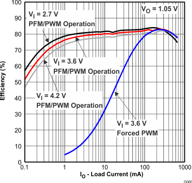
TPS62671 TPS62672 TPS62674 TPS62675 TPS626751 TPS626765 TPS62679 eff3_io_lvs952.gif
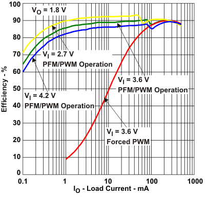
Figure 1. Efficiency vs Load Current
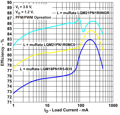
TPS62671 TPS62672 TPS62674 TPS62675 TPS626751 TPS626765 TPS62679 TPS626765_Efficiency.gif
Figure 3. Efficiency vs Load Current
TPS62671 TPS62672 TPS62674 TPS62675 TPS626751 TPS626765 TPS62679 eff4a_io_lvs952.gif
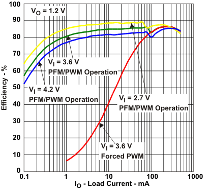
Figure 5. Efficiency vs Load Current
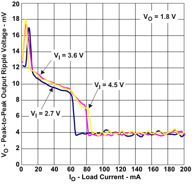
TPS62671 TPS62672 TPS62674 TPS62675 TPS626751 TPS626765 TPS62679 vo2_io2_lvs952.gif
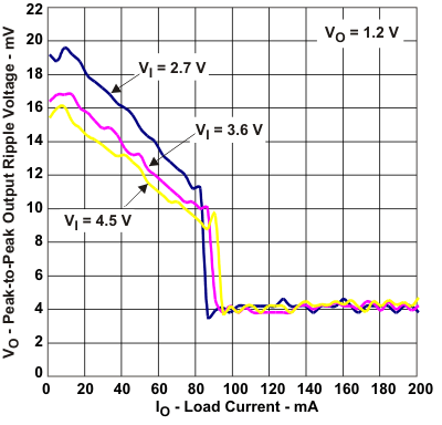
Figure 7. Peak-To-Peak Output Ripple Voltage vs Load Current
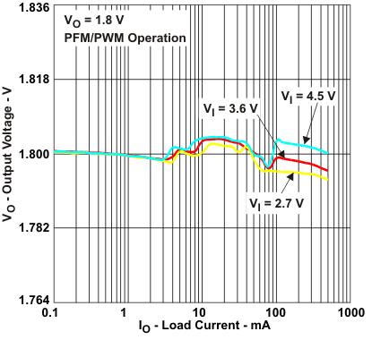
TPS62671 TPS62672 TPS62674 TPS62675 TPS626751 TPS626765 TPS62679 voc_io_lvs952.gif
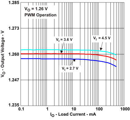
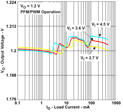
Figure 9. DC Output Voltage vs Load Current
TPS62671 TPS62672 TPS62674 TPS62675 TPS626751 TPS626765 TPS62679 vo2_io_lvs952.gif
Figure 11. DC Output Voltage vs Load Current
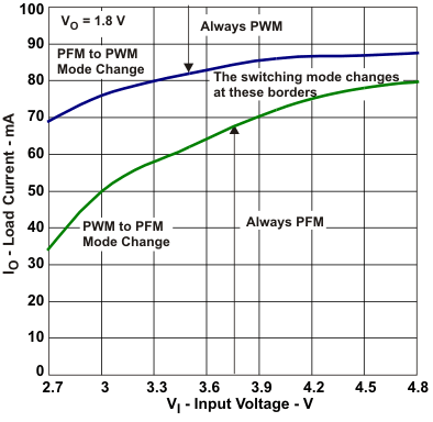
TPS62671 TPS62672 TPS62674 TPS62675 TPS626751 TPS626765 TPS62679 io2_vi2_lvs952.gif
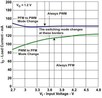
Figure 13. PFM/PWM Boundaries
TPS62671 TPS62672 TPS62674 TPS62675 TPS626751 TPS626765 TPS62679 fs_vi_lvs952.gif
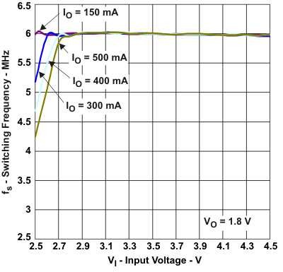
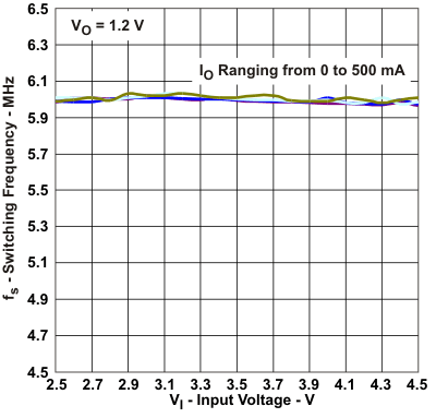
Figure 15. PWM Switching Frequency vs Input Voltage
TPS62671 TPS62672 TPS62674 TPS62675 TPS626751 TPS626765 TPS62679 pfm_swfreq_lvs952.gif
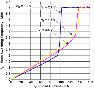
Figure 17. PFM Switching Frequency vs Input Voltage
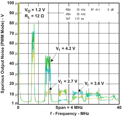
TPS62671 TPS62672 TPS62674 TPS62675 TPS626751 TPS626765 TPS62679 onois_pwm1_lvs952.gif
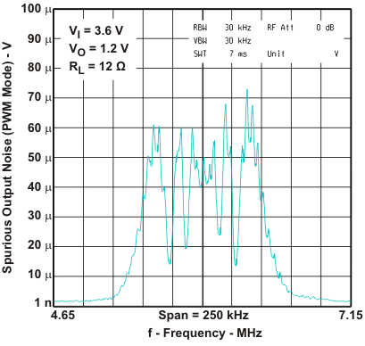
Figure 19. Spurious Output Noise (PWM Mode) vs Frequency
TPS62671 TPS62672 TPS62674 TPS62675 TPS626751 TPS626765 TPS62679 onois_pfm_lvs952.gif
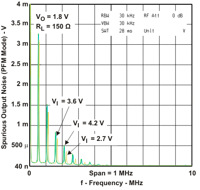
Figure 21.
TPS62671 TPS62672 TPS62674 TPS62675 TPS626751 TPS626765 TPS62679 spec_noiseden_lvs952.gif
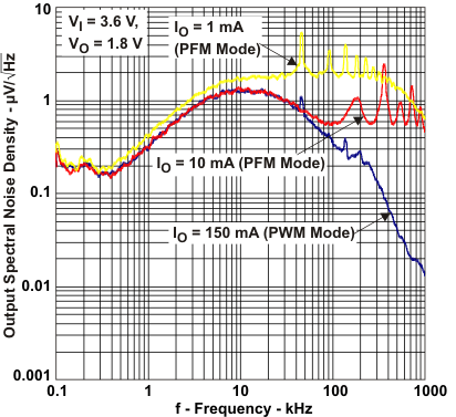
Figure 23. Output Spectral Noise Density vs Frequency
TPS62671 TPS62672 TPS62674 TPS62675 TPS626751 TPS626765 TPS62679 eff_io_lvs952.gif
Figure 2. Efficiency vs Load Current
TPS62671 TPS62672 TPS62674 TPS62675 TPS626751 TPS626765 TPS62679 eff4_io_lvs952.gif
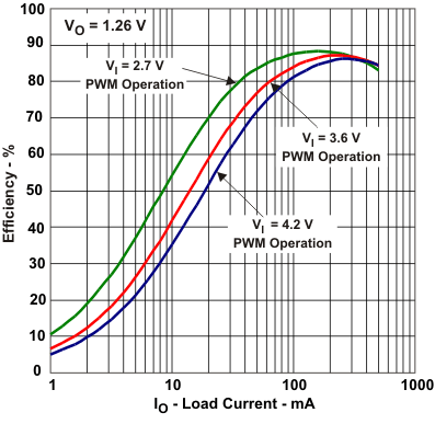
Figure 4. Efficiency vs Load Current
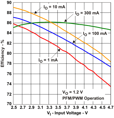
TPS62671 TPS62672 TPS62674 TPS62675 TPS626751 TPS626765 TPS62679 new_eff_vi_lvs952.gif
Figure 6. Efficiency vs Input Voltage
TPS62671 TPS62672 TPS62674 TPS62675 TPS626751 TPS626765 TPS62679 vo_io_lvs952.gif
Figure 8. Peak-To-Peak Output Ripple Voltage vs Load Current
TPS62671 TPS62672 TPS62674 TPS62675 TPS626751 TPS626765 TPS62679 voa_io_lvs952.gif
Figure 10. DC Output Voltage vs Load Current
TPS62671 TPS62672 TPS62674 TPS62675 TPS626751 TPS626765 TPS62679 io_vi_lvs952.gif
Figure 12. PFM/PWM Boundaries
TPS62671 TPS62672 TPS62674 TPS62675 TPS626751 TPS626765 TPS62679 iq1_vi_lvs952.gif
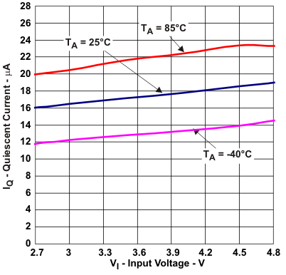
Figure 14. Quiescent Current vs Input Voltage
TPS62671 TPS62672 TPS62674 TPS62675 TPS626751 TPS626765 TPS62679 fs2_vi_lvs952.gif
Figure 16. PWM Switching Frequency vs Input Voltage
TPS62671 TPS62672 TPS62674 TPS62675 TPS626751 TPS626765 TPS62679 PSRR1_f_lvs952.gif
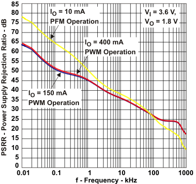
Figure 18. PSRR vs Frequency
TPS62671 TPS62672 TPS62674 TPS62675 TPS626751 TPS626765 TPS62679 onois_pwm2_lvs952.gif
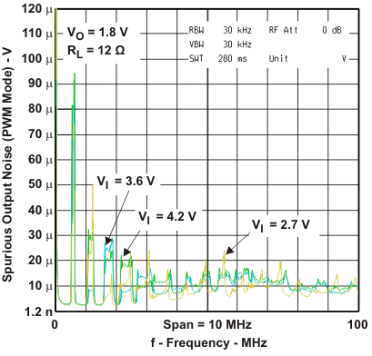
Figure 20. Spurious Output Noise (PWM Mode) vs Frequency
TPS62671 TPS62672 TPS62674 TPS62675 TPS626751 TPS626765 TPS62679 onois_pwm3_lvs952.gif
Figure 22.