SLVSEC6D June 2019 – March 2020 TPS62840
PRODUCTION DATA.
- 1 Features
- 2 Applications
- 3 Description
- 4 Revision History
- 5 Device Comparison Table
- 6 Pin Configuration and Functions
- 7 Specifications
-
8 Detailed Description
- 8.1 Overview
- 8.2 Functional Block Diagram
- 8.3
Feature Description
- 8.3.1 Smart Enable and Shutdown
- 8.3.2 Soft Start
- 8.3.3 Mode Selection: Power-Save Mode (PFM/PWM) or Forced PWM Operation (FPWM)
- 8.3.4 Output Voltage Selection (VSET)
- 8.3.5 Undervoltage Lockout UVLO
- 8.3.6 Switch Current Limit / Short Circuit Protection
- 8.3.7 Output Voltage Discharge
- 8.3.8 Thermal Shutdown
- 8.3.9 STOP Mode
- 8.4 Device Functional Modes
- 9 Application and Implementation
- 10Power Supply Recommendations
- 11Layout
- 12Device and Documentation Support
- 13Mechanical, Packaging, and Orderable Information
Package Options
Mechanical Data (Package|Pins)
Thermal pad, mechanical data (Package|Pins)
- DLC|8
Orderable Information
8.3.2 Soft Start
To protect the battery and system from excessive inrush current, the device features a soft start of the output voltage.
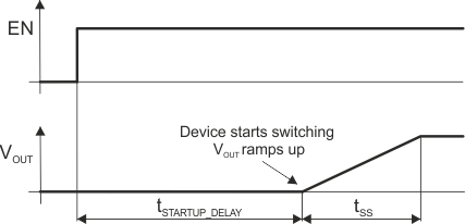
Once the device has been enabled, it initializes and powers up its internal circuits. This occurs during the regulator start-up delay time (tSTARTUP_DELAY). Once this delay expires, the device enters soft start, starts switching, and ramps up the output voltage.
The device operates with a reduced switch current limit (ILIMF_SS) throughout the entire soft-start phase (tSS). The switch current limit is increased to its nominal value (ILIMF) once the output voltage has reached its nominal value or the reduced current limit soft-start time (tSS_ILIMF) has expired, whichever occurs first. The soft-start phase (tSS) can last up to approximately 700 µs. Figure 12 shows the start-up procedure.
 Figure 12. Device Start-up