SLVSEW4 April 2019 TPS650002-Q1
PRODUCTION DATA.
- 1 Features
- 2 Applications
- 3 Description
- 4 Revision History
- 5 Pin Configuration and Functions
- 6 Specifications
- 7 Detailed Description
- 8 Application and Implementation
- 9 Power Supply Recommendations
- 10Layout
- 11Device and Documentation Support
- 12Mechanical, Packaging, and Orderable Information
Package Options
Mechanical Data (Package|Pins)
- RTE|16
Thermal pad, mechanical data (Package|Pins)
- RTE|16
Orderable Information
7.3.1 Step-Down Converter
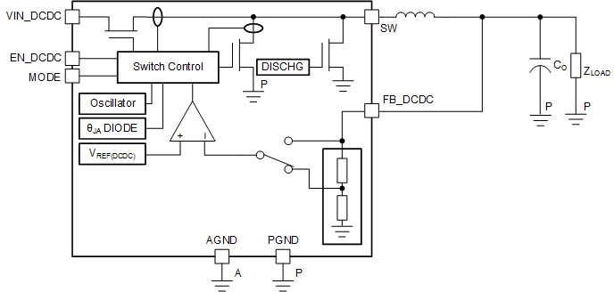
The step-down converter is intended to allow maximum flexibility in the end equipment. Figure 16 shows the necessary connections.
 Figure 16. DC-DC Converter Block Diagram
 Externally adjustable output voltages and additional current-limit options are also possible. Contact TI for further information.
The step-down converter has two modes of operation to maximize efficiency at different load conditions. At moderate to heavy load currents, the device operates in a fixed-frequency pulse-width modulation (PWM) mode that results in small output ripple and high efficiency. Pulling the MODE pin to a DC-high level results in PWM mode over the entire load range.
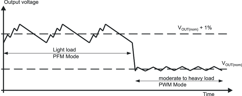
At light load currents, the device operates in a pulsed frequency-modulation (PFM) mode to improve efficiency. The transition to this mode occurs when the inductor current through the low-side FET becomes zero, indicating discontinuous conduction. PFM mode also results in the output voltage increasing by 1% from the PWM mode value. This voltage positioning is intended to minimize both the voltage undershoot of a load step from light to heavy loads, as when a processor moves from sleep to active modes, and the voltage overshoot at load removal. shows the voltage positioning behavior for a light-to-heavy load step.
 Figure 17. PFM Voltage Positioning
 Pulling the MODE pin to DC ground results in an automatic transition between PFM and PWM modes to maximize efficiency.
The DC-DC converter output automatically discharges to ground through an internal 450-Ω load when EN_DCDC goes low or when the UVLO condition is met.