SLVSEW4 April 2019 TPS650002-Q1
PRODUCTION DATA.
- 1 Features
- 2 Applications
- 3 Description
- 4 Revision History
- 5 Pin Configuration and Functions
- 6 Specifications
- 7 Detailed Description
- 8 Application and Implementation
- 9 Power Supply Recommendations
- 10Layout
- 11Device and Documentation Support
- 12Mechanical, Packaging, and Orderable Information
Package Options
Mechanical Data (Package|Pins)
- RTE|16
Thermal pad, mechanical data (Package|Pins)
- RTE|16
Orderable Information
6.7 Typical Characteristics
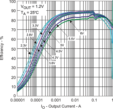 Figure 1. Efficiency (DC-DC 600-mA PFM Mode)
vs Output Current
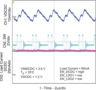 Figure 3. Output Voltage Ripple (DC-DC PFM Mode)
 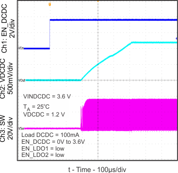 Figure 5. Start-Up Timing (DC-DC)
 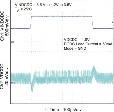 Figure 7. Line Transient Response (DC-DC PFM Mode)
 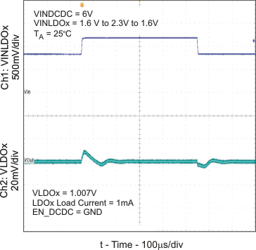 Figure 9. Line Transient Response (LDOx)
 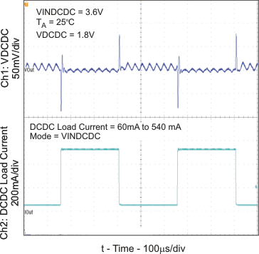 Figure 11. Load Transient Response (DC-DC PWM Mode)
 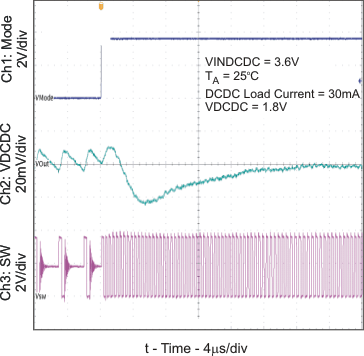 Figure 13. PFM to PWM Transition (DC-DC)
 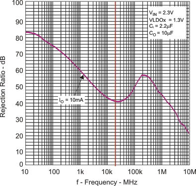 Figure 15. Power-Supply Rejection Ratio (LDOx) vs Frequency
 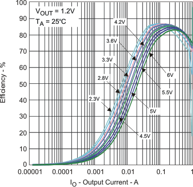 Figure 2. Efficiency (DC-DC 600-mA PWM Mode)
vs Output Current
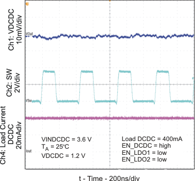 Figure 4. Output Voltage Ripple (DC-DC PWM Mode)
 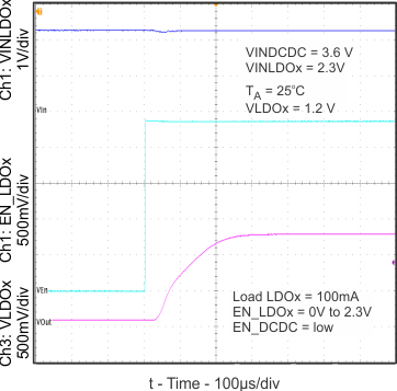 Figure 6. Start-Up Timing (LDOx)
 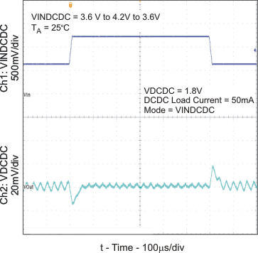 Figure 8. Line Transient Response (DC-DC PWM Mode)
 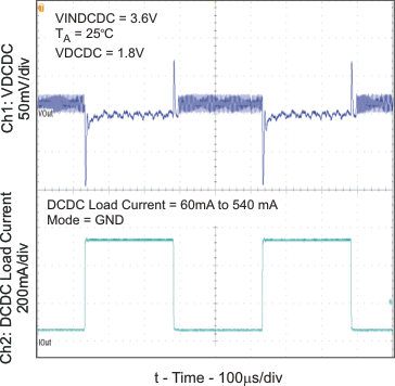 Figure 10. Load Transient Response (DC-DC PFM Mode)
 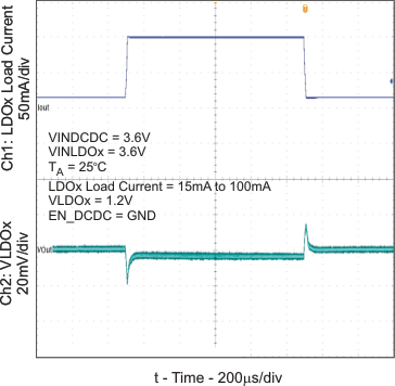 Figure 12. Load Transient Response (LDOx)
 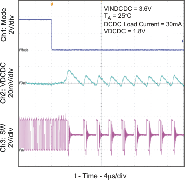 Figure 14. PWM to PFM Transition (DC-DC)