SLVS754D March 2007 – January 2015 TPS65053
PRODUCTION DATA.
- 1 Features
- 2 Applications
- 3 Description
- 4 Revision History
- 5 Pin Configuration and Functions
- 6 Specifications
-
7 Detailed Description
- 7.1 Overview
- 7.2 Functional Block Diagrams
- 7.3 Feature Description
- 7.4 Device Functional Modes
-
8 Application and Implementation
- 8.1 Application Information
- 8.2
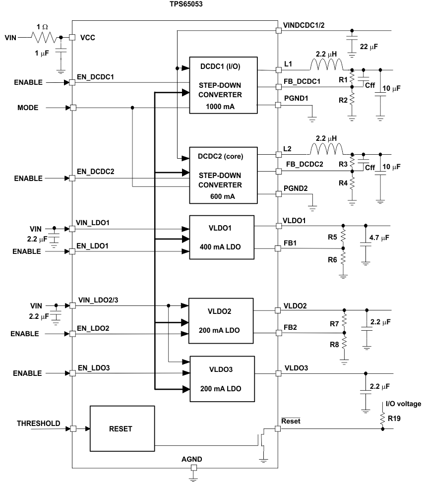
Typical Application
- 8.2.1 Design Requirements
- 8.2.2 Detailed Design Procedure
- 8.2.3 Application Curves
- 9 Power Supply Recommendations
- 10Layout
- 11Device and Documentation Support
- 12Mechanical, Packaging, and Orderable Information
Package Options
Mechanical Data (Package|Pins)
- RGE|24
Thermal pad, mechanical data (Package|Pins)
- RGE|24
Orderable Information
1 Features
- Up To 95% Efficiency
- Output Current for DC-DC Converters:
- TPS65053: DCDC1 = 1 A; DCDC2 = 0.6 A
- TPS650531, TPS650532: DCDC1 = 1 A; DCDC2 = 1 A
- TPS65058: DCDC1 = 0.6 A; DCDC2 = 1 A
- TPS65053, TPS650531, TPS650532: DC-DC Converters Externally Adjustable
- TPS65058: DCDC1 Fixed at 3.3V, DCDC2 selectable between 1.8V and 1.2V with Dynamic Voltage Scaling for Core Processor Supply
- VIN Range for DC-DC Converters
From 2.5 V to 6 V - 2.25-MHz Fixed Frequency Operation
- Power Save Mode at Light Load Current
- 180° Out-of-Phase Operation
- Output Voltage Accuracy in PWM Mode ±1%
- Total Typical 32-μA Quiescent Current for Both DC-DC Converters
- 100% Duty Cycle for Lowest Dropout
- One General-Purpose 400-mA LDO
- Two General-Purpose 200-mA LDOs
- VIN Range for LDOs from 1.5 V to 6.5 V
- Output Voltage for LDOs:
- TPS65053 / TPS650531 / TPS650532: VLDO1 and VLDO2 Externally Adjustable, VLDO3 = 1.3 V / 1.2 V / 1.5 V
- TPS65058: VLDO1 = 3.3 V, VLDO2 selectable between 1.8V and 1.2V, VLDO2 selectable between 1.8V and 1.3V
2 Applications
- Cell Phones, Smart Phones
- WLAN
- PDAs, Pocket PCs, GPS
- OMAP™ and Low-Power DSP Supply
- Portable Media Players
- Digital Cameras
- Satellite Radio Modules
3 Description
The TPS6505xx family of devices are integrated power management ICs for applications powered by one Li-Ion or Li-Polymer cell, which require multiple power rails. The TPS6505xx devices provide two highly efficient, 2.25-MHz step-down converters targeted at providing the core voltage and I/O voltage in a processor-based system. Both step-down converters enter a low power mode at light load for maximum efficiency across the widest possible range of load currents. For low noise applications the devices can be forced into fixed frequency PWM mode by pulling the MODE pin high. The TPS6505xx devices also integrate one 400-mA LDO and two 200-mA LDO voltage regulators. Each LDO operates with an input voltage range between 1.5 V and 6.5 V allowing them to be supplied from one of the step-down converters or directly from the main battery.
Device Information(1)
| PART NUMBER | PACKAGE | BODY SIZE (NOM) |
|---|---|---|
| TPS65053 | VQFN (24) | 4.00 mm x 4.00 mm |
| TPS650531 | ||
| TPS650532 | ||
| TPS65058 |
- For all available packages, see the orderable addendum at the end of the datasheet.
Typical Application Schematic