SLVSC01A June 2013 – April 2015 TPS65133
PRODUCTION DATA.
- 1 Features
- 2 Applications
- 3 Description
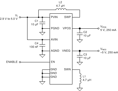
- 4 Typical Application
- 5 Revision History
- 6 Pin Configuration and Functions
- 7 Specifications
- 8 Detailed Description
- 9 Application and Implementation
- 10Power Supply Recommendations
- 11Layout
- 12Device and Documentation Support
- 13Mechanical, Packaging, and Orderable Information
Package Options
Mechanical Data (Package|Pins)
- DPD|12
Thermal pad, mechanical data (Package|Pins)
- DPD|12
Orderable Information
1 Features
- 2.9-V to 5.0-V Input Voltage Range
- Fixed 5.0-V Positive Output Voltage (VPOS)
- Fixed –5.0-V Negative Output Voltage (VNEG)
- ±1% Output Voltage Accuracy
- High Efficiency
- 250-mA Output Current Capability
- Independent Converter Operation Allows 100% Output Current Mismatch
- Excellent Line and Load Transient Response
- Operates in CCM to Minimize Output Noise
- Boost Converter able to Operate with Input Supply Voltages close to 5.0 V
- Short-Circuit Protection
- Thermal Shutdown
2 Applications
- LCD Bias
- AMOLED Supplies
- Operational Amplifier Supplies
- Headphone Amplifier Supplies
- Sensor Front-End Supplies
- Data Acquisition Supplies
- General ±5-V Power Supplies
3 Description
The TPS65133 is designed to supply any system requiring ±5.0-V supply rails. Each output can supply up to 250 mA of output current. The input supply voltage range is suitable for use with lithium ion batteries or from a fixed 3.3-V supply.
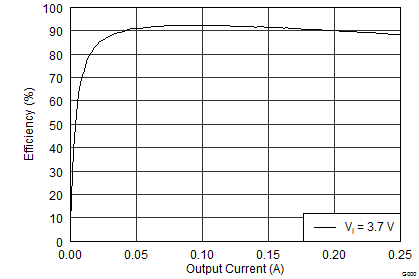
Efficiency is typically over 90% for most applications (operating from a lithium ion battery, output currents in the range 50 mA to 200 mA). The two converters in the TPS65133 device operate independently, allowing 100% mismatch between positive and negative output currents.
Device Information(1)
| PART NUMBER | PACKAGE | BODY SIZE (NOM) |
|---|---|---|
| TPS65133 | WSON (12) | 3.00 mm × 3.00 mm |
- For all available packages, see the orderable addendum at the end of the datasheet.

