SLDS234B December 2017 – September 2018 TPS65218D0
UNLESS OTHERWISE NOTED, this document contains PRODUCTION DATA.
- 1 Device Overview
- 2 Revision History
- 3 Pin Configuration and Functions
- 4 Specifications
-
5 Detailed Description
- 5.1 Overview
- 5.2 Functional Block Diagram
- 5.3
Feature Description
- 5.3.1
Wake-Up and Power-Up and Power-Down Sequencing
- 5.3.1.1 Power-Up Sequencing
- 5.3.1.2 Power-Down Sequencing
- 5.3.1.3 Strobes 1 and 2
- 5.3.1.4 Supply Voltage Supervisor and Power Good (PGOOD)
- 5.3.1.5 Backup Supply Power-Good (PGOOD_BU)
- 5.3.1.6 Internal LDO (INT_LDO)
- 5.3.1.7 Current Limited Load Switches
- 5.3.1.8 LDO1
- 5.3.1.9 Coin Cell Battery Voltage Acquisition
- 5.3.1.10 UVLO
- 5.3.1.11 Power-Fail Comparator
- 5.3.1.12 Battery-Backup Supply Power-Path
- 5.3.1.13 DCDC3 / DCDC4 Power-Up Default Selection
- 5.3.1.14 I/O Configuration
- 5.3.1.15 Push Button Input (PB)
- 5.3.1.16 AC_DET Input (AC_DET)
- 5.3.1.17 Interrupt Pin (INT)
- 5.3.1.18 I2C Bus Operation
- 5.3.1
Wake-Up and Power-Up and Power-Down Sequencing
- 5.4 Device Functional Modes
- 5.5 Programming
- 5.6
Register Maps
- 5.6.1 Password Protection
- 5.6.2 Freshness Seal (FSEAL) Bit
- 5.6.3 FLAG Register
- 5.6.4
TPS65218D0 Registers
- 5.6.4.1 CHIPID Register (subaddress = 0x0) [reset = 0x5]
- 5.6.4.2 INT1 Register (subaddress = 0x1) [reset = 0x0]
- 5.6.4.3 INT2 Register (subaddress = 0x2) [reset = 0x0]
- 5.6.4.4 INT_MASK1 Register (subaddress = 0x3) [reset = 0x0]
- 5.6.4.5 INT_MASK2 Register (subaddress = 0x4) [reset = 0x0]
- 5.6.4.6 STATUS Register (subaddress = 0x5) [reset = 00XXXXXXb]
- 5.6.4.7 CONTROL Register (subaddress = 0x6) [reset = 0x0]
- 5.6.4.8 FLAG Register (subaddress = 0x7) [reset = 0x0]
- 5.6.4.9 PASSWORD Register (subaddress = 0x10) [reset = 0x0]
- 5.6.4.10 ENABLE1 Register (subaddress = 0x11) [reset = 0x0]
- 5.6.4.11 ENABLE2 Register (subaddress = 0x12) [reset = 0x0]
- 5.6.4.12 CONFIG1 Register (subaddress = 0x13) [reset = 0x4C]
- 5.6.4.13 CONFIG2 Register (subaddress = 0x14) [reset = 0xC0]
- 5.6.4.14 CONFIG3 Register (subaddress = 0x15) [reset = 0x0]
- 5.6.4.15 DCDC1 Register (offset = 0x16) [reset = 0x99]
- 5.6.4.16 DCDC2 Register (subaddress = 0x17) [reset = 0x99]
- 5.6.4.17 DCDC3 Register (subaddress = 0x18) [reset = 0x8C]
- 5.6.4.18 DCDC4 Register (subaddress = 0x19) [reset = 0xB2]
- 5.6.4.19 SLEW Register (subaddress = 0x1A) [reset = 0x6]
- 5.6.4.20 LDO1 Register (subaddress = 0x1B) [reset = 0x1F]
- 5.6.4.21 SEQ1 Register (subaddress = 0x20) [reset = 0x0]
- 5.6.4.22 SEQ2 Register (subaddress = 0x21) [reset = 0x0]
- 5.6.4.23 SEQ3 Register (subaddress = 0x22) [reset = 0x98]
- 5.6.4.24 SEQ4 Register (subaddress = 0x23) [reset = 0x75]
- 5.6.4.25 SEQ5 Register (subaddress = 0x24) [reset = 0x12]
- 5.6.4.26 SEQ6 Register (subaddress = 0x25) [reset = 0x63]
- 5.6.4.27 SEQ7 Register (subaddress = 0x26) [reset = 0x3]
- 6 Application and Implementation
- 7 Power Supply Recommendations
- 8 Layout
- 9 Device and Documentation Support
- 10Mechanical, Packaging, and Orderable Information
Package Options
Mechanical Data (Package|Pins)
Thermal pad, mechanical data (Package|Pins)
Orderable Information
5.3.1.3 Strobes 1 and 2
STROBE1 and STROBE2 are dedicated to DCDC5 and DCDC6 which are always-on; powered up as soon as the device exits the OFF state, and ON in any other state. STROBE 1 and 2 options are available only for DCDC5 and DCDC6, not for any other rails.
STROBE 1 and STROBE 2 occur in every power-up sequence, regardless if the rail is already powered up. If the rail is not to be powered up, its respective strobe setting must be set to 0x00.
When a power-down sequence initiates, STROBE1 and STROBE2 occur only if the FSEAL bit is 0b. Otherwise, both strobes are omitted and DCDC5 and DCDC6 maintain state.
NOTE
The power-down sequence follows the reverse of the power-up sequence. STROBE2 and STROBE1 are executed only if FSEAL bit is 0b.
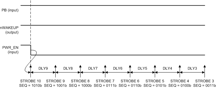
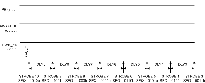
 Figure 5-4 Power-Down Sequences to OFF State;
PWR_EN is Power-Down Event; FSEAL = 0b

PWR_EN is Power-Down Event; FSEAL = 1b

TSD or UV is Power-Down Event; FSEAL = 1b