SLVSAE1B October 2010 – September 2015 TPS65708
PRODUCTION DATA.
- 1 Features
- 2 Applications
- 3 Description
- 4 Revision History
- 5 Pin Configuration and Functions
- 6 Specifications
- 7 Parameter Measurement Information
-
8 Detailed Description
- 8.1 Overview
- 8.2 Functional Block Diagram
- 8.3
Feature Description
- 8.3.1 DC-DC Converters
- 8.3.2 Power Save Mode
- 8.3.3 Dynamic Voltage Positioning
- 8.3.4 Soft Start
- 8.3.5 100% Duty Cycle Low Dropout Operation
- 8.3.6 180° Out-of-Phase Operation
- 8.3.7 Undervoltage Lockout and Enable for DCDC1, DCDC2, LDO1, and LDO2
- 8.3.8 Output Voltage Discharge
- 8.3.9 Power-Up Sequencing
- 8.3.10 Short-Circuit Protection
- 8.3.11 Thermal Shutdown
- 8.3.12 LDOs
- 8.3.13 LED Driver
- 8.4 Device Functional Modes
- 9 Application and Implementation
- 10Power Supply Recommendations
- 11Layout
- 12Device and Documentation Support
- 13Mechanical, Packaging, and Orderable Information
Package Options
Mechanical Data (Package|Pins)
- YZH|16
Thermal pad, mechanical data (Package|Pins)
Orderable Information
1 Features
- Two 400-mA Step-Down Converters
- Up to 95% Efficiency
- VIN Range for DC-DC Converters From
3.6 V to 6 V - 2.25-MHz Fixed-Frequency Operation
- Power Save Mode at Light Load Current
- Output Voltage Accuracy in PWM mode ±1.5%
- 100% Duty Cycle for Lowest Dropout
- 180° Out-of-Phase Operation
- 2 General Purpose 200-mA LDOs
- LDOs Optionally Powered From Step-Down Converters
- 7.5-mA PWM Dimmable Current Sink
- Available in a 16-Ball DSBGA (WCSP) With
0.5-mm Pitch - Device Options:
- VDCDC1 = 3.3 V
- VDCDC2 = 1.8 V
- VLDO1 = 2.8 V
- VLDO2 = 1.2 V
- ISINK(PWM=1) = 7.5 mA
- SEQUENCING : DCDC1, LDO1, DCDC2, LDO2
2 Applications
- Monitors
- Laptops
- Handheld Equipment
3 Description
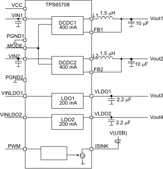
The TPS65708 device is a power management unit targeted for embedded camera modules or other portable low-power consumer end equipment. The device contains two high-efficiency step-down converters, two low-dropout linear regulators, and a 7.5-mA current sink for driving a LED. The 2.25-MHz step-down converter enters a low-power mode at light load for maximum efficiency across the widest possible range of load currents. For low-noise applications, the devices can be forced into fixed-frequency PWM mode using the MODE pin. The device allows the use of small inductors and capacitors to achieve a small solution size. The TPS65708 device provides an output current of up to 400 mA on both DC-DC converters and up to 200 mA on each of the LDOs. The enable signal to the DC-DC converters and LDOs is generated internally by the undervoltage lockout circuit.
The TPS65708 comes in a small 16-pin wafer chip-scale package (WCSP) with 0.5-mm ball pitch.
Device Information(1)
| PART NUMBER | PACKAGE | BODY SIZE (NOM) |
|---|---|---|
| TPS65708 | DSBGA (16) | 2.00 mm × 2.00 mm |
- For all available packages, see the orderable addendum at the end of the data sheet.
Application Circuit
