SLIS165G December 2014 – February 2019 TPS659037
PRODUCTION DATA.
- 1 Device Overview
- 2 Revision History
- 3 Pin Configuration and Functions
-
4 Specifications
- 4.1 Absolute Maximum Ratings
- 4.2 ESD Ratings
- 4.3 Recommended Operating Conditions
- 4.4 Thermal Information
- 4.5 Electrical Characteristics: Latch Up Rating
- 4.6 Electrical Characteristics: LDO Regulator
- 4.7 Electrical Characteristics: Dual-Phase (SMPS12 and SMPS45) and Triple-Phase (SMPS123 and SMPS457) Regulators
- 4.8 Electrical Characteristics: Stand-Alone Regulators (SMPS3, SMPS6, SMPS7, SMPS8, and SMPS9)
- 4.9 Electrical Characteristics: Reference Generator (Bandgap)
- 4.10 Electrical Characteristics: 16-MHz Crystal Oscillator, 32-kHz RC Oscillator, and Output Buffers
- 4.11 Electrical Characteristics: DC-DC Clock Sync
- 4.12 Electrical Characteristics: 12-Bit Sigma-Delta ADC
- 4.13 Electrical Characteristics: Thermal Monitoring and Shutdown
- 4.14 Electrical Characteristics: System Control Threshold
- 4.15 Electrical Characteristics: Current Consumption
- 4.16 Electrical Characteristics: Digital Input Signal Parameters
- 4.17 Electrical Characteristics: Digital Output Signal Parameters
- 4.18 Electrical Characteristics: I/O Pullup and Pulldown
- 4.19 I2C Interface Timing Requirements
- 4.20 SPI Timing Requirements
- 4.21 Typical Characteristics
-
5 Detailed Description
- 5.1 Overview
- 5.2 Functional Block Diagram
- 5.3
Feature Description
- 5.3.1 Power Management
- 5.3.2
Power Resources (Step-Down and Step-Up SMPS Regulators, LDOs)
- 5.3.2.1
Step-Down Regulators
- 5.3.2.1.1 Sync Clock Functionality
- 5.3.2.1.2 Output Voltage and Mode Selection
- 5.3.2.1.3 Current Monitoring and Short Circuit Detection
- 5.3.2.1.4 POWERGOOD
- 5.3.2.1.5 DVS-Capable Regulators
- 5.3.2.1.6 Non DVS-Capable Regulators
- 5.3.2.1.7 Step-Down Converters SMPS12 and SMPS123
- 5.3.2.1.8 Step-Down Converter SMPS45 and SMPS457
- 5.3.2.1.9 Step-Down Converters SMPS3, SMPS6, SMPS7, SMPS8, and SMPS9
- 5.3.2.2 LDOs – Low Dropout Regulators
- 5.3.2.1
Step-Down Regulators
- 5.3.3 Long-Press Key Detection
- 5.3.4 RTC
- 5.3.5 GPADC – 12-Bit Sigma-Delta ADC
- 5.3.6 General-Purpose I/Os (GPIO Pins)
- 5.3.7 Thermal Monitoring
- 5.3.8 Interrupts
- 5.3.9 Control Interfaces
- 5.3.10 Device Identification
- 5.4 Device Functional Modes
-
6 Application and Implementation
- 6.1 Application Information
- 6.2
Typical Application
- 6.2.1 Design Requirements
- 6.2.2 Detailed Design Procedure
- 6.2.3 Application Curves
- 7 Power Supply Recommendations
- 8 Layout
- 9 Device and Documentation Support
- 10Mechanical, Packaging, and Orderable Information
Package Options
Mechanical Data (Package|Pins)
- ZWS|169
Thermal pad, mechanical data (Package|Pins)
Orderable Information
5.3.2.1.4 POWERGOOD
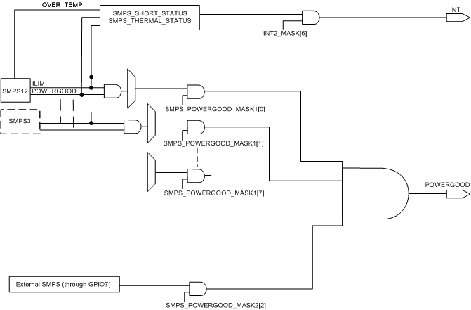
The external POWERGOOD pin indicates if the outputs of the SMPS are correct or not (Figure 5-3). Either voltage and current monitoring or a current monitoring only can be selected for POWERGOOD indication. This selection is common for all SMPSs in the
SMPS_POWERGOOD_MASK2.POWERGOOD_TYPE_SELECT bit register. When both voltage and current are monitored, POWERGOOD signal active (polarity is programmable) indicates that all SMPS outputs are within certain percentage, VSMPSPG , of the programmed value and that load current is below ILIM.
All POWERGOOD sources can be masked in the SMPS_POWERGOOD_MASK1 and
SMPS_POWERGOOD_MASK2 registers. By default, only the SMPS12 rail (or SMPS123 rail if in triple phase) is monitored. When an SMPS is disabled, it should be masked to prevent it forcing POWERGOOD inactive. When SMPS voltage is transitioning from one target voltage to another due to DVS command, voltage monitoring is internally masked and POWERGOOD is not impacted.
Including POWERGOOD in the GPADC result is possible for SMPS output current monitoring by setting SMPS_COMPMODE = 1. Only one SMPS can be monitored by the GPADC channel at the time.
The POWERGOOD function can also be used for monitoring an external SMPS is at the correct output level and the load is lower than the current limit; indication is through the GPIO_7 pin.
All POWERGOOD sources can be masked in SMPS_POWERGOOD_MASK1 and
SMPS_POWERGOOD_MASK2 registers.
CAUTION
The current monitor on multi-phase rails (such as SMPS12, SMPS123, or SMPS45) may cause POWERGOOD to change to a low level (with default polarity) when transitioning from multi-phase operation to single phase operation. TI recommends masking the multi-phase rails as a POWERGOOD source, using SMPS_POWERGOOD_MASK1, or debouncing the POWERGOOD signal if this POWERGOOD toggle is not desired in the application design.
 Figure 5-3 POWERGOOD Block Diagram