SLVSCK1A April 2014 – April 2014 TPS65980
PRODUCTION DATA.
- 1 Features
- 2 Applications
- 3 Description
- 4 Simplified Schematic
- 5 Revision History
- 6 Pin Configuration and Functions
- 7 Specifications
- 8 Detailed Description
- 9 Application and Implementation
- 10Power Supply Recommendations
- 11Layout
- 12Device and Documentation Support
- 13Mechanical, Packaging, and Orderable Information
Package Options
Mechanical Data (Package|Pins)
- RHF|24
Thermal pad, mechanical data (Package|Pins)
Orderable Information
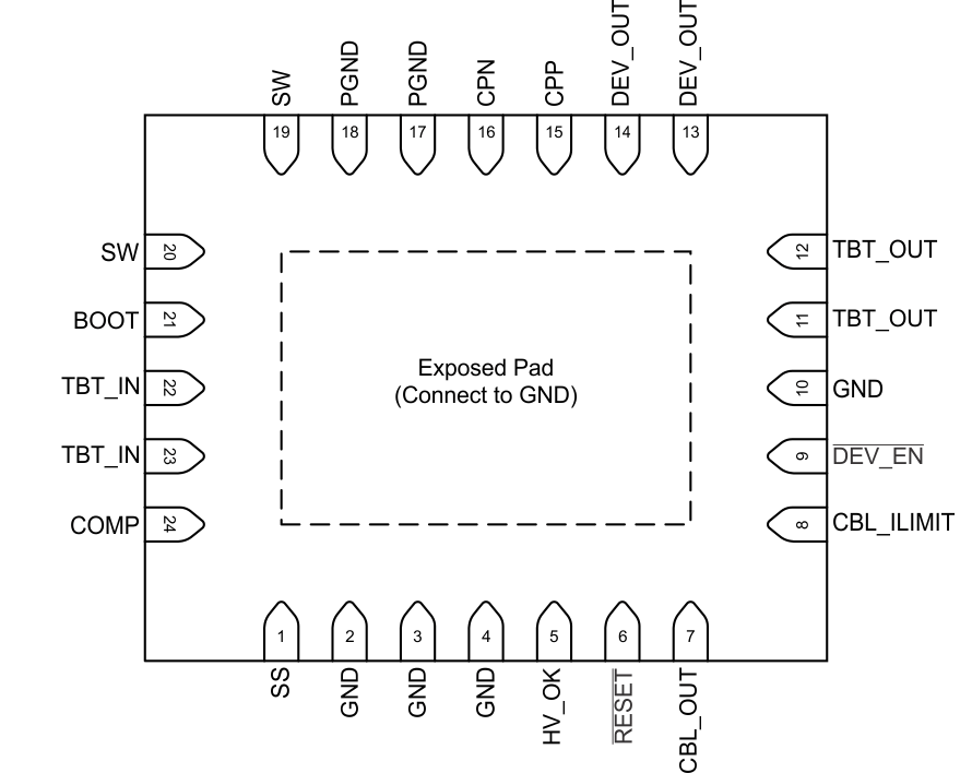
6 Pin Configuration and Functions
VQFN (RHF) 24-Pin
TOP VIEW
VQFN (RHF) 24-Pin
BOTTOM
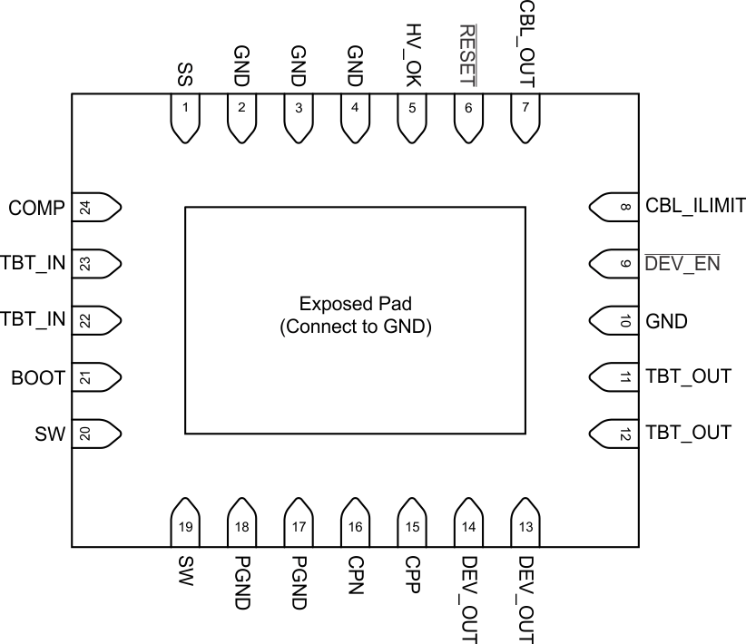
Pin Functions
| PIN | I/O | DESCRIPTION | |
|---|---|---|---|
| NO. | NAME | ||
| 1 | SS | ANALOG | Soft Start Capacitance. This pin sets the soft start ramp rate when the TBT_IN voltage ramps from 0V to high voltage. |
| 2, 3, 4 | GND | GND | Device Ground |
| 5 | HV_OK | OUTPUT | High Voltage Present Indicator. This pin indicates that a high voltage is present on TBT_IN. The output asserts high when the TBT_IN pin is above the VHVT voltage and the RESET output is asserting high. |
| 6 | RESET | OUTPUT | Reset output indicator. This pin asserts low when TBT_OUT is in under-voltage. |
| 7 | CBL_OUT | PWROUT | Current Limited Power Output to Thunderbolt™ Cable. This pin supplies power to the Thunderbolt™ cable. The current limit of this pin is set by the CBL_ILIMIT pin. |
| 8 | CBL_ILIMIT | INPUT | Current Limit Set. Logic input that sets the current limit state on the CBL_OUT pin. Tie pin to TBT_OUT for a logic high input. |
| 9 | DEV_EN | INPUT | Device Enable Input. When input pin is high, DEV_OUT is high impedance. When input pin low, DEV_OUT is connected to TBT_OUT. |
| 10 | GND | ANALOG | Device Ground |
| 11, 12 | TBT_OUT | PWROUT | Power Output to Thunderbolt™ circuitry. This pin supplies power to the Thunderbolt™ controller. |
| 13, 14 | DEV_OUT | PWROUT | Power Output to peripheral device. This pin supplies power to circuitry not associated with the Thunderbolt™ controller or the Thunderbolt™ cable. It is intended to supply power to the peripheral device main function. |
| 15 | CPP | ANALOG | Charge Pump Capacitance Positive Output |
| 16 | CPN | ANALOG | Charge Pump Capacitance Negative Output |
| 17, 18 | PGND | GND | Buck Controller Power Ground |
| 19, 20 | SW | ANALOG | Buck Controller Switch Output |
| 21 | BOOT | ANALOG | Buck Controller Bootstrap |
| 22, 23 | TBT_IN | PWRIN | Power Input from Thunderbolt™ Cable. This pin is the power supply to the device. |
| 24 | COMP | ANALOG | Buck Converter Compensation. This pin provides compensation to the buck converter feedback loop. |