SBVS066R December 2005 – April 2017 TPS74401
PRODUCTION DATA.
- 1 Features
- 2 Applications
- 3 Description
- 4 Revision History
- 5 Pin Configuration and Functions
- 6 Specifications
- 7 Detailed Description
- 8 Application and Implementation
- 9 Power Supply Recommendations
- 10Layout
- 11Device and Documentation Support
- 12Mechanical, Packaging, and Orderable Information
Package Options
Mechanical Data (Package|Pins)
Thermal pad, mechanical data (Package|Pins)
Orderable Information
8 Application and Implementation
NOTE
Information in the following applications sections is not part of the TI component specification, and TI does not warrant its accuracy or completeness. TI’s customers are responsible for determining suitability of components for their purposes. Customers should validate and test their design implementation to confirm system functionality.
8.1 Application Information
The TPS74401 belongs to a family of ultra-low dropout regulators that feature soft-start. These regulators use a low current bias input to power all internal control circuitry, allowing the NMOS pass transistor to regulate very low output voltages with low VIN to VOUT headroom.
The use of an NMOS-pass FET offers several critical advantages for many applications. Unlike a PMOS topology device, the output capacitor has little affect on loop stability. This architecture allows the TPS74401 to be stable with any or even no output capacitor. Transient response is also superior to PMOS topologies, particularly for low VIN applications.
The TPS74401 features a programmable, voltage-controlled soft-start circuit that provides a smooth, monotonic start-up and limits startup inrush currents that can be caused by large capacitive loads. A power-good (PG) output is available to allow supply monitoring and sequencing of other supplies. An enable (EN) pin with hysteresis and de-glitch allows slow-ramping signals to be used for sequencing the device. The low VIN and VOUT capability allows for inexpensive, easy-to-design, and efficient linear regulation between the multiple supply voltages often present in processor intensive systems.
8.1.1 Input, Output, and Bias Capacitor Requirements
The TPS74401 does not require any output capacitor for stability. If an output capacitor is needed, the device is designed to be stable for all available types and values of output capacitance. The device is also stable with multiple capacitors in parallel, of any type or value. This flexibility is a result of an innovative control loop that ensures the device is stable independent of the output capacitance.
The capacitance required on the IN and BIAS pins strongly depends on the input supply source impedance. To counteract any inductance in the input, the minimum recommended capacitor for VIN and VBIAS is 1 μF. If VIN and VBIAS are connected to the same supply, the recommended minimum capacitor for VBIAS is 4.7 μF. Use good quality, low-ESR capacitors on the input; ceramic X5R and X7R capacitors are preferred. Place these capacitors as close to the pins as possible for optimum performance and to help ensure stability.
8.1.2 Transient Response
The TPS74401 is designed to have transient response within 5% for most applications without an output capacitor. In some cases, the transient response can be limited by the transient response of the input supply. This limitation is especially true in applications where the difference between the input and output is less than 300 mV. In this case, adding additional input capacitance improves the transient response much more than just adding additional output capacitance. With a solid input supply, adding additional output capacitance reduces undershoot and overshoot during a transient at the expense of a slightly longer VOUT recovery time; see Figure 20 in the Typical Characteristics section. Because the TPS74401 is stable without an output capacitor, many applications can allow for little or no capacitance at the LDO output. For these applications, local bypass capacitance for the device under power can be sufficient to meet the transient requirements of the application. This design reduces the total solution cost by avoiding the need to use expensive, high-value capacitors at the LDO output.
8.1.3 Dropout Voltage
The TPS74401 offers industry-leading dropout performance, making the device well-suited for high-current, low VIN and low VOUT applications. The extremely low dropout of the TPS74401 also allows the device to be used in place of a dc/dc converter and also achieve good efficiencies. Equation 3 provides a quick estimate of the efficiencies.

This efficiency allows users to redesign the power architecture for their applications to achieve the smallest, simplest, and lowest cost solution.
There are two different specifications for dropout voltage with the TPS74401. The first specification (see Figure 38) is referred to as VIN Dropout and is for users who wish to apply an external bias voltage to achieve low dropout. This specification assumes that VBIAS is at least 1.62 V above VOUT; for example, when VBIAS is powered by a 3.3-V rail with 5% tolerance and with VOUT = 1.5 V. If VBIAS is higher than (3.3 V × 0.95) or VOUT is less than 1.5 V, VIN dropout is less than specified.
The second specification (see Figure 39) is referred to as VBIAS Dropout and is for users who wish to have VBIAS < VIN + 1.62 V. This option allows the device to be used in applications where an auxiliary bias voltage is not available or low dropout is not required. Dropout is limited by BIAS in these applications because VBIAS provides the gate drive to the pass FET and therefore must be greater than VOUT + VDO (VBIAS). Because of this usage, IN and BIAS tied together easily consume excessive power. Pay attention and do not exceed the power rating of the IC package.
8.1.4 Output Noise
The TPS74401 provides low output noise when a soft-start capacitor is used. When the device reaches the end of the soft-start cycle, the soft-start capacitor serves as a filter for the internal reference. By using a 0.001-μF soft-start capacitor, the output noise is reduced by half and is typically 19 μVRMS for a 1.2-V output (100 Hz to 100 kHz). Noise is a function of the set output voltage because most of the output noise is generated by the internal reference. The RMS noise with a 0.001-μF soft-start capacitor is given in Equation 4.

The low output noise of the TPS74401 makes the device a good choice for powering transceivers, PLLs, or other noise-sensitive circuitry.
8.2 Typical Applications
8.2.1 Setting the TPS74401
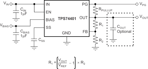
Figure 27 shows a typical application circuit for the TPS74401.
R1 and R2 can be calculated for any output voltage using the formula shown in Figure 27. Table 3 lists sample resistor values of common output voltages. In order to achieve the maximum accuracy specifications, R2 must be ≤ 4.99 kΩ.
Table 3. Standard 1% Resistor Values for Programming the Output Voltage(1)
| R1 (kΩ) | R2 (kΩ) | VOUT (V) |
|---|---|---|
| Short | Open | 0.8 |
| 0.619 | 4.99 | 0.9 |
| 1.13 | 4.53 | 1.0 |
| 1.37 | 4.42 | 1.05 |
| 1.87 | 4.99 | 1.1 |
| 2.49 | 4.99 | 1.2 |
| 4.12 | 4.75 | 1.5 |
| 3.57 | 2.87 | 1.8 |
| 3.57 | 1.69 | 2.5 |
| 3.57 | 1.15 | 3.3 |
NOTE
When VBIAS and VEN are present and VIN is not supplied, this device outputs approximately 50 μA of current from OUT. Although this condition does not cause any damage to the device, the output current can charge up the OUT node if total resistance between OUT and GND (including external feedback resistors) is greater than 10 kΩ.
8.2.1.1 Design Requirements
The design goals are VIN = 1.8 V, VOUT = 1.5 V, and IOUT = 2 A max. The design optimizes transient response while meeting a 1-ms startup time with a startup dominated by the soft-start feature. The input supply comes from a supply on the same circuit board. The available system rails for VBIAS are 2.7 V, 3.3 V, and 5 V.
The design space consists of CIN, COUT, CBIAS, CSS, VBIAS, R1, R2, and R3, and the circuit is from Figure 27.
This example uses a VIN of 1.8 V, with a VBIAS of 2.5 V.
8.2.1.2 Detailed Design Procedure
The first step for this design is to examine the maximum load current along with the input and output voltage requirements, to determine if the device thermal and dropout voltage requirements can be met. At 3 A, the input dropout voltage of the TPS74401 family is a maximum of 240 mV over temperature. As a result, the dropout headroom is sufficient for operation over both input and output voltage accuracy.
The maximum power dissipated in the linear regulator is the maximum voltage dropped across the pass element from the input to the output multiplied by the maximum load current. In this example, the maximum voltage drop across in the pass element is (1.8 V – 1.5 V), giving a VDROP = 300 mV. The power dissipated can than be estimated by the equation PDISS = IL(max) × VDROP = ~600 mW. This calculation gives an efficiency of nearly 83.3% by using Equation 3.
When the power dissipated in the linear regulator is known, the corresponding junction temperature increase can be calculated. To estimate the junction temperature increase above ambient, the power dissipated must be multiplied by the junction-to-ambient thermal resistance. For thermal resistance information, refer to the Thermal Information table. For this example, using the KTW package, the junction temperature rise is calculated to be 21.2°C. The maximum junction temperature increase is calculated by adding the junction temperature rise to the maximum ambient temperature. In this example, the maximum junction temperature is 46.2°C. Keep in mind that the junction temperature must be less than 125°C for reliable operation. Additional ground planes, added thermal vias, and air flow all help to improve the thermal transfer characteristics of the system.
The next step is to determine the bias voltage or if a separate source is needed for the bias voltage. Because VIN is less than VOUT plus the VBIAS dropout, VBIAS must be an independent supply. VBIAS = VOUT + 1.62 V = 3.12 V; the system has a 3.3-V rail to use for this supply and also to provide some limited headroom for VBIAS. The 5-V rail is a better choice to improve the performance of the LDO, so the 5-V rail is used.
8.2.1.3 Application Curves
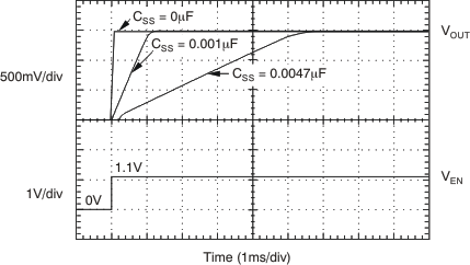 Figure 28. Turn-On Response
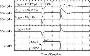 Figure 30. Load Transient Response
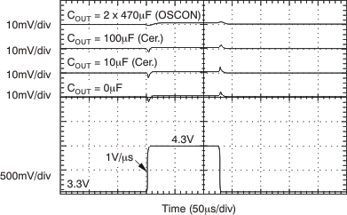 Figure 32. VBIAS Line Transient (3 A)
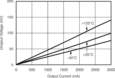 Figure 34. VIN Dropout Voltage vs IOUT and Temperature (TJ)
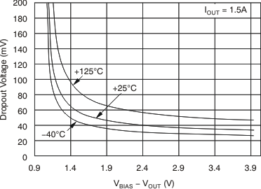 Figure 36. VIN Dropout Voltage vs VBIAS – VOUT and Temperature (TJ)
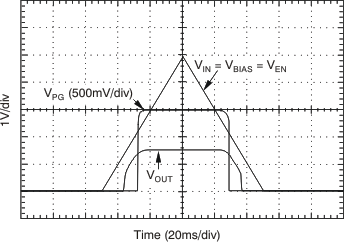 Figure 29. Power-Up, Power-Down
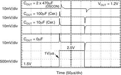 Figure 31. VIN Line Transient (3 A)
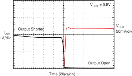 Figure 33. Output Short-Circuit Recovery
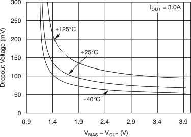 Figure 35. VIN Dropout Voltage vs VBIAS – VOUT and Temperature (TJ)
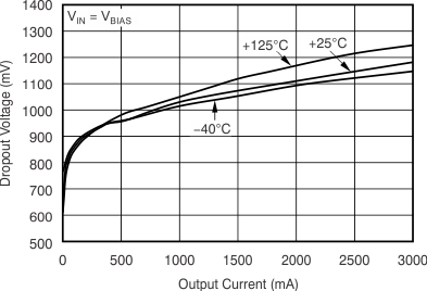 Figure 37. VBIAS Dropout Voltage vs IOUT and Temperature (TJ)
8.2.2 Using an Auxiliary Bias Rail
Figure 38 shows a typical application of the TPS74401 using an auxiliary bias rail. The auxiliary bias rail allows for the designer to specify the system to have a low VDO. The bias rail supplies the error amplifier with a higher supply voltage, increasing the voltage that can be applied to the gate of the pass device.
VBIAS must be at least VOUT + 1.62 V.
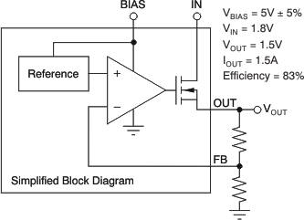 Figure 38. Typical Application of the TPS74401 Using an Auxiliary Bias Rail
8.2.3 Without an Auxiliary Bias
The TPS74401 family is capable of operating without a bias rail if VIN ≥ VOUT + VDO (VBIAS). Additional capacitance is advised for this scenario, with at least 4.7 µF of capacitance near the input pin. Figure 39 shows a typical application of the TPS74401 without an auxiliary bias.
If using the TPS74401 in this situation and under high load conditions, ensure that the printed circuit board (PCB) provides adequate thermal handling capabilities to keep the device in its recommended operating range. See the Power Supply Recommendations section for more information.
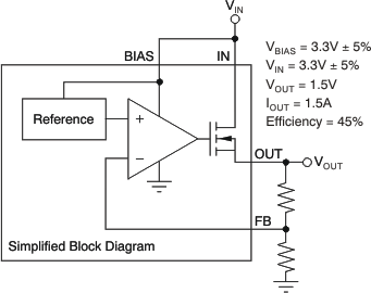 Figure 39. Typical Application of the TPS74401 Without an Auxiliary Bias
