SBVS066R December 2005 – April 2017 TPS74401
PRODUCTION DATA.
- 1 Features
- 2 Applications
- 3 Description
- 4 Revision History
- 5 Pin Configuration and Functions
- 6 Specifications
- 7 Detailed Description
- 8 Application and Implementation
- 9 Power Supply Recommendations
- 10Layout
- 11Device and Documentation Support
- 12Mechanical, Packaging, and Orderable Information
Package Options
Mechanical Data (Package|Pins)
Thermal pad, mechanical data (Package|Pins)
Orderable Information
7 Detailed Description
7.1 Overview
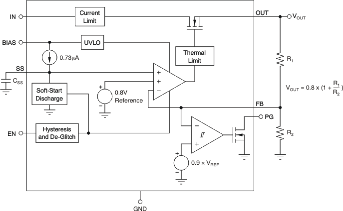
The TPS74401 family of low-dropout regulators (LDOs) incorporates many features to ensure a wide range of uses. Hysteresis and de-glitch on the EN input improve the ability to sequence multiple devices without worrying about false start-up. The soft-start is fully programmable and allows the user to control the startup time of the LDO output. Hysteresis is also available on the PG comparator to ensure no false PG signals. The TPS74401 family of LDOs is ideal for FPGAs, DSPs, and any other device that requires linear supply and sequencing.
7.3 Feature Description
7.3.1 Enable, Shutdown
The enable (EN) pin is active high and compatible with standard digital signaling levels. VEN lower than 0.4 V turns the regulator off, whereas VEN above 1.1 V turns the regulator on. Unlike many regulators, the enable circuitry has hysteresis and de-glitching for use with relatively slow-ramping analog signals. This configuration allows the TPS74401 to be enabled by connecting the output of another supply to the EN pin. The enable circuitry typically has 50 mV of hysteresis and a de-glitch circuit to help avoid on-off cycling resulting from small glitches in the VEN signal.
The enable threshold is typically 0.8 V and varies with temperature and process variations. Temperature variation is approximately –1 mV/°C; therefore, process variation accounts for most of the variation in the enable threshold. If precise turn-on timing is required, use a fast rise-time signal to enable the TPS74401.
If not used, EN can be connected to either IN or BIAS. If EN is connected to IN, connect EN as close as possible to the largest capacitance on the input to prevent voltage droops on that line from triggering the enable circuit.
7.3.2 Power-Good (VQFN Package Only)
The power-good (PG) pin is an open-drain output and can be connected to any 5.5 V or lower rail through an external pullup resistor. This pin requires at least 1.1 V on VBIAS in order to have a valid output. The PG output is high-impedance when VOUT is greater than (VIT + VHYS). If VOUT drops below VIT or if VBIAS drops below 1.9 V, the open-drain output turns on and pulls the PG output low. The PG pin also asserts when the device is disabled. The recommended operating condition of the PG pin sink current is up to 1 mA, thus the pullup resistor for PG must be in the range of 10 kΩ to 1 MΩ. PG is only provided on the VQFN package. If output voltage monitoring is not needed, the PG pin can be left floating.
7.3.3 Internal Current Limit
The TPS74401 features a factory-trimmed, accurate current limit that is flat over temperature and supply voltage. The current limit allows the device to supply surges of up to 3.5 A and maintain regulation. The current limit responds in approximately 10 μs to reduce the current during a short-circuit fault. Recovery from a short-circuit condition is well-controlled and results in very little output overshoot when the load is removed. See Figure 25 in the Typical Characteristics section for short-circuit recovery performance.
The internal current limit protection circuitry of the TPS74401 is designed to protect against overload conditions. This circuitry is not intended to allow operation above the rated current of the device. Continuously running the TPS74401 above the rated current degrades device reliability.
7.3.4 Thermal Protection
Thermal protection disables the output when the junction temperature rises to approximately 155°C, allowing the device to cool. When the junction temperature cools to approximately 140°C, the output circuitry is enabled. Depending on power dissipation, thermal resistance, and ambient temperature the thermal protection circuit can cycle on and off. This cycling limits the dissipation of the regulator, protecting it from damage as a result of overheating.
Activation of the thermal protection circuit indicates excessive power dissipation or inadequate heatsinking. For reliable operation, limit junction temperature to 125°C maximum. To estimate the margin of safety in a complete design (including heatsink), increase the ambient temperature until thermal protection is triggered; use worst-case loads and signal conditions. For good reliability, trigger thermal protection at least 30°C above the maximum expected ambient condition of the application. This condition produces a worst-case junction temperature of 125°C at the highest expected ambient temperature and worst-case load.
The internal protection circuitry of the TPS74401 is designed to protect against overload conditions. This circuitry is not intended to replace proper heatsinking. Continuously running the TPS74401 into thermal shutdown degrades device reliability.
7.4 Device Functional Modes
7.4.1 Normal Operation
The device regulates to the nominal output voltage under the following conditions:
- The input voltage and bias voltage are both at least at the respective minimum specifications.
- The enable voltage has previously exceeded the enable rising threshold voltage and has not decreased below the enable falling threshold.
- The output current is less than the current limit.
- The device junction temperature is less than the maximum specified junction temperature.
- The device is not operating in dropout.
7.4.2 Dropout Operation
If the input voltage is lower than the nominal output voltage plus the specified dropout voltage, but all other conditions are met for normal operation, the device operates in dropout mode. In this condition, the output voltage is the same as the input voltage minus the dropout voltage. The transient performance of the device is significantly degraded because the pass device is in a triode state and no longer controls the current through the LDO. Line or load transients in dropout can result in large output voltage deviations.
7.4.3 Disabled
The device is disabled under the following conditions:
- The input or bias voltages are below the respective minimum specifications.
- The enable voltage is less than the enable falling threshold voltage or has not yet exceeded the enable rising threshold.
- The device junction temperature is greater than the thermal shutdown temperature.
Table 1 shows the conditions that lead to the different modes of operation.
Table 1. Device Functional Mode Comparison
| OPERATING MODE | PARAMETER | ||||
|---|---|---|---|---|---|
| VIN | VEN | VBIAS | IOUT | TJ | |
| Normal mode | VIN > VOUT(nom) + VDO (VIN) | VEN > VEN(high) | VBIAS ≥ VOUT + 1.62 V | I OUT < ICL | T J < 125°C |
| Dropout mode | VIN < VOUT(nom) + VDO (VIN) | VEN > VEN(high) | VBIAS < VOUT + 1.62 V | — | TJ < 125°C |
| Disabled mode (any true condition disables the device) |
VIN < VIN(min) | VEN < VEN(low) | VBIAS < VBIAS(min) | — | TJ > 155°C |
7.5 Programming
7.5.1 Programmable Soft-Start
The TPS74401 features a programmable, monotonic, voltage-controlled soft-start that is set with an external capacitor (CSS). This feature is important for many applications to eliminate power-up initialization problems when powering FPGAs, DSPs, or other processors. The controlled voltage ramp of the output also reduces peak inrush current during start-up, minimizing start-up transients to the input power bus.
To achieve a linear and monotonic soft-start, the TPS74401 error amplifier tracks the voltage ramp of the external soft-start capacitor until the voltage exceeds the internal reference. The soft-start ramp time depends on the soft-start charging current (ISS), the soft-start capacitance (CSS), and the internal reference voltage (VREF), and can be calculated using Equation 1:

If large output capacitors are used, the device current limit (ICL) and the output capacitor can set the start-up time. In this case, the start-up time is given by Equation 2:

where
- VOUT(nom) is the nominal set output voltage as set by the user,
- COUT is the output capacitance,
- and ICL(min) is the minimum current limit for the device.
In applications where monotonic startup is required, the soft-start time given by Equation 1 must be set to be greater than Equation 2.
The maximum recommended soft-start capacitor is 0.015 μF. Larger soft-start capacitors can be used and do not damage the device; however, the soft-start capacitor discharge circuit may not be able to fully discharge the soft-start capacitor when re-enabled. Soft-start capacitors larger than 0.015 μF can be a problem in applications where the user must rapidly pulse the enable pin and also require the device to soft-start from ground. CSS must be low-leakage; X7R, X5R, or C0G dielectric materials are preferred. Table 2 lists suggested soft-start capacitor values.
Table 2. Standard Capacitor Values for Programming the Soft-Start Time(1)
| CSS | SOFT-START TIME |
|---|---|
| Open | 0.1 ms |
| 470 pF | 0.5 ms |
| 1000 pF | 1 ms |
| 4700 pF | 5 ms |
| 0.01 μF | 10 ms |
| 0.015 μF | 16 ms |
7.5.2 Sequencing Requirements
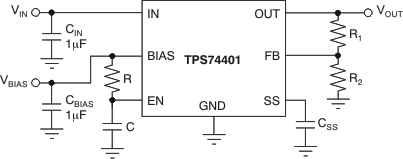
The device can have VIN, VBIAS, and VEN sequenced in any order without causing damage to the device. However, for the soft-start function to work as intended, certain sequencing rules must be applied. Enabling the device after VIN and VBIAS are present is preferred, and can be accomplished using a digital output from a processor or supply supervisor. An analog signal from an external RC circuit, as shown in Figure 26, can also be used as long as the delay time is long enough for VIN and VBIAS to be present.
 Figure 26. Soft-Start Delay Using an RC Circuit on Enable
If a signal is not available to enable the device after IN and BIAS, simply connecting EN to IN is acceptable for most applications as long as VIN is greater than 1.1 V and the ramp rate of VIN and VBIAS is faster the set soft-start ramp rate. If the ramp rate of the input sources is slower than the set soft-start time, the output tracks the slower supply less the dropout voltage until the set output voltage is reached. If EN is connected to BIAS, the device soft-starts as programmed, provided that VIN is present before VBIAS. If VBIAS and VEN are present before VIN is applied and the set soft-start time has expired, then VOUT tracks VIN.

