SLVS181J December 1998 – September 2019 TPS763
PRODUCTION DATA.
- 1 Features
- 2 Applications
- 3 Description
- 4 Revision History
- 5 Pin Configuration and Functions
- 6 Specifications
- 7 Detailed Description
- 8 Application and Implementation
- 9 Power Supply Recommendations
- 10Layout
- 11Device and Documentation Support
- 12Mechanical, Packaging, and Orderable Information
Package Options
Refer to the PDF data sheet for device specific package drawings
Mechanical Data (Package|Pins)
- DBV|5
Thermal pad, mechanical data (Package|Pins)
Orderable Information
8.2.2.2 Output Voltage Programming
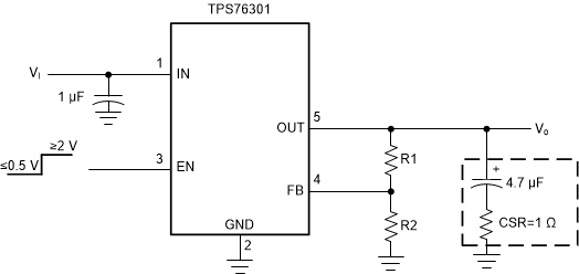
The output voltage of the TPS76301 adjustable regulator is programmed using an external resistor divider as shown in Figure 21. The output voltage is calculated using Equation 1.
Equation 1. 

where
- Vref = 1.192 V typical (the internal reference voltage)
- 0.995 is a constant used to center the load regulator (1%)
Resistors R1 and R2 must be chosen for approximately 7-µA divider current. Lower value resistors can be used but offer no inherent advantage and waste more power. Higher values must be avoided as leakage currents at FB increase the output voltage error. TI recommends choosing a design procedure of R2 = 169 kΩ to set the divider current at 7 µA and then calculate R1 using Equation 2.
Equation 2. 

 Figure 21. TPS76301 Adjustable LDO Regulator Programming