SLVS348L July 2001 – May 2015 TPS793
PRODUCTION DATA.
- 1 Features
- 2 Applications
- 3 Description
- 4 Revision History
- 5 Pin Configuration and Functions
- 6 Specifications
- 7 Detailed Description
- 8 Application and Implementation
- 9 Power Supply Recommendations
- 10Layout
- 11Device and Documentation Support
- 12Mechanical, Packaging, and Orderable Information
Package Options
Mechanical Data (Package|Pins)
Thermal pad, mechanical data (Package|Pins)
Orderable Information
7 Detailed Description
7.1 Overview
The TPS793 family of LDO regulators has been optimized for use in noise-sensitive battery-operated equipment. The device features extremely low dropout voltages, high PSRR, ultralow output noise, low quiescent current (170 μA typically), and enable-input to reduce supply currents to less than 1 μA when the regulator is turned off.
7.2 Functional Block Diagrams
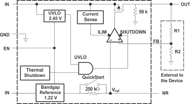
 Figure 21. TPS79301 Block Diagram (Adjustable Version)
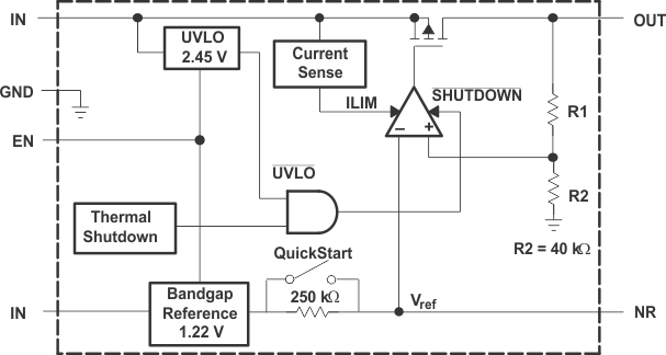
 Figure 22. TPS793 Block Diagram (Fixed Version)
7.3 Feature Description
7.3.1 Undervoltage Lockout (UVLO)
The TPS793 uses an undervoltage lockout (UVLO) circuit that disables the output until the input voltage is greater than the rising UVLO voltage. This circuit ensures that the device does not exhibit any unpredictable behavior when the supply voltage is lower than the operational range of the internal circuitry, VIN(min).
7.3.2 Shutdown
The enable pin (EN) is active high. Enable the device by forcing the EN pin to exceed VEN(high) (1.7 V, minimum). Turn off the device by forcing the EN pin to drop below 0.7 V. If shutdown capability is not required, connect EN to IN.
7.3.3 Foldback Current Limit
The TPS793 features internal current limiting and thermal protection. During normal operation, the TPS793 limits output current to approximately 400 mA. When current limiting engages, the output voltage scales back linearly until the overcurrent condition ends. While current limiting is designed to prevent gross device failure, care should be taken not to exceed the power dissipation ratings of the package or the absolute maximum voltage ratings of the device.
7.3.4 Thermal Protection
Thermal protection disables the output when the junction temperature rises to approximately 165°C, allowing the device to cool. When the junction temperature cools to approximately 140°C, the output circuitry is again enabled. Depending on power dissipation, thermal resistance, and ambient temperature, the thermal protection circuit may cycle on and off. This cycling limits regulator dissipation, protecting the device from damage as a result of overheating.
Any tendency to activate the thermal protection circuit indicates excessive power dissipation or an inadequate heatsink. For reliable operation, junction temperature must be limited to 125°C maximum. To estimate the margin of safety in a complete design (including heatsink), increase the ambient temperature until the thermal protection is triggered; use worst-case loads and signal conditions.
The TPS793 internal protection circuitry is designed to protect against overload conditions. This circuitry is not intended to replace proper heatsinking. Continuously running the TPS793 into thermal shutdown degrades device reliability.
7.3.5 Reverse Current Operation
The TPS793 PMOS-pass transistor has a built-in back diode that conducts reverse current when the input voltage drops below the output voltage (for example, during power down). Current is conducted from the output to the input and is not internally limited. If extended reverse voltage operation is anticipated, external limiting to 5% of the rated output current is recommended.
7.4 Device Functional Modes
7.4.1 Normal Operation
The device regulates to the nominal output voltage under the following conditions:
- The input voltage is at least as high as VIN(min).
- The input voltage is greater than the nominal output voltage added to the dropout voltage.
- The enable voltage is greater than VEN(min).
- The output current is less than the current limit.
- The device junction temperature is less than the maximum specified junction temperature.
7.4.2 Dropout Operation
If the input voltage is lower than the nominal output voltage plus the specified dropout voltage, but all other conditions are met for normal operation, the device operates in dropout mode. In this mode of operation, the output voltage is the same as the input voltage minus the dropout voltage. The transient performance of the device is significantly degraded because the pass device is in the linear region and no longer controls the current through the LDO. Line or load transients in dropout can result in large output voltage deviations.
7.4.3 Disabled
The device is disabled under the following conditions:
- The enable voltage is less than the enable falling threshold voltage or has not yet exceeded the enable rising threshold.
- The device junction temperature is greater than the thermal shutdown temperature.
- The input voltage is less than UVLOfalling.
Table 1 shows the conditions that lead to the different modes of operation.
Table 1. Device Functional Mode Comparison
| OPERATING MODE | PARAMETER | |||
|---|---|---|---|---|
| VIN | VEN | IOUT | TJ | |
| Normal mode | VIN > VOUT(nom) + VDO and VIN > VIN(min) |
VEN > VEN(high) | IOUT < ILIM | TJ < 125°C |
| Dropout mode | VIN(min) < VIN < VOUT(nom) + VDO | VEN > VEN(high) | — | TJ < 125°C |
| Disabled mode (any true condition disables the device) |
VIN < UVLOfalling | VEN < VEN(low) | — | TJ > 165°C(1) |