SBVS342A February   2019  – March 2019 TPS7A16A-Q1

PRODUCTION DATA.  

  1. Features
  2. Applications
  3. Description
    1.     Typical Application Schematic
  4. Revision History
  5. Pin Configuration and Functions
    1.     Pin Functions
  6. Specifications
    1. 6.1 Absolute Maximum Ratings
    2. 6.2 ESD Ratings
    3. 6.3 Recommended Operating Conditions
    4. 6.4 Thermal Information
    5. 6.5 Electrical Characteristics
    6. 6.6 Typical Characteristics
  7. Detailed Description
    1. 7.1 Overview
    2. 7.2 Functional Block Diagram
    3. 7.3 Feature Description
      1. 7.3.1 Enable (EN)
      2. 7.3.2 Regulated Output (VOUT)
      3. 7.3.3 PG Delay Timer (DELAY)
    4. 7.4 Device Functional Modes
      1. 7.4.1 Power-Good
        1. 7.4.1.1 Power-Good Delay and Delay Capacitor
  8. Application and Implementation
    1. 8.1 Application Information
    2. 8.2 Typical Applications
      1. 8.2.1 TPS7A16A-Q1 Circuit as an Adjustable Regulator
        1. 8.2.1.1 Design Requirements
        2. 8.2.1.2 Detailed Design Procedure
          1. 8.2.1.2.1 Adjustable Voltage Operation
            1. 8.2.1.2.1.1 Resistor Selection
          2. 8.2.1.2.2 Capacitor Recommendations
          3. 8.2.1.2.3 Input and Output Capacitor Requirements
          4. 8.2.1.2.4 Feed-Forward Capacitor (Only for Adjustable Version)
          5. 8.2.1.2.5 Transient Response
        3. 8.2.1.3 Application Curves
      2. 8.2.2 Automotive Applications
        1. 8.2.2.1 Design Requirements
        2. 8.2.2.2 Detailed Design Procedure
          1. 8.2.2.2.1 Device Recommendations
        3. 8.2.2.3 Application Curves
  9. Power Supply Recommendations
  10. 10Layout
    1. 10.1 Layout Guidelines
      1. 10.1.1 Additional Layout Considerations
      2. 10.1.2 Power Dissipation
      3. 10.1.3 Thermal Considerations
    2. 10.2 Layout Examples
  11. 11Device and Documentation Support
    1. 11.1 Receiving Notification of Documentation Updates
    2. 11.2 Community Resources
    3. 11.3 Trademarks
    4. 11.4 Electrostatic Discharge Caution
    5. 11.5 Glossary
  12. 12Mechanical, Packaging, and Orderable Information

Package Options

Mechanical Data (Package|Pins)
Thermal pad, mechanical data (Package|Pins)
Orderable Information

Typical Characteristics

at TA = –40°C to 125°C, VIN = VOUT(NOM) + 0.5 V or VIN = 3 V (whichever is greater), VEN = VIN, IOUT = 10 µA, CIN = 1 µF, COUT = 2.2 µF, and FB tied to OUT (unless otherwise noted)
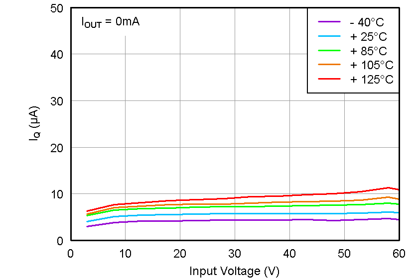
TPS7A16A-Q1 tc_iq-vin_bvs171.png
Figure 1. Quiescent Current vs Input Voltage
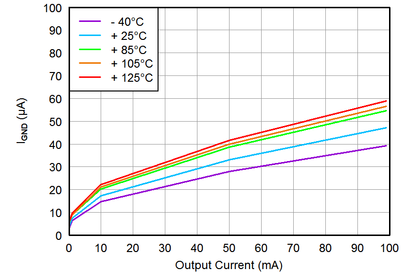
TPS7A16A-Q1 tc_ignd-io_bvs171.png
Figure 3. Quiescent Current vs Output Current
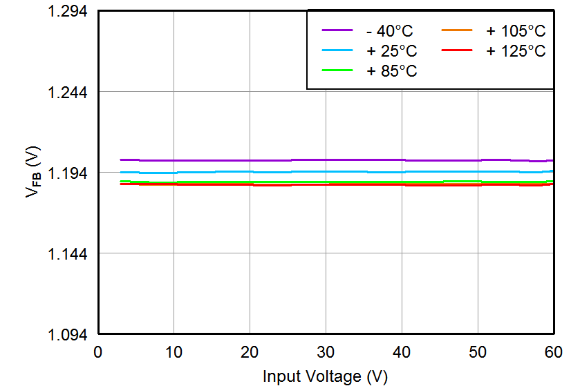
TPS7A16A-Q1 tc_vfb-vin_bvs171.png
Figure 5. Feedback Voltage vs Input Voltage
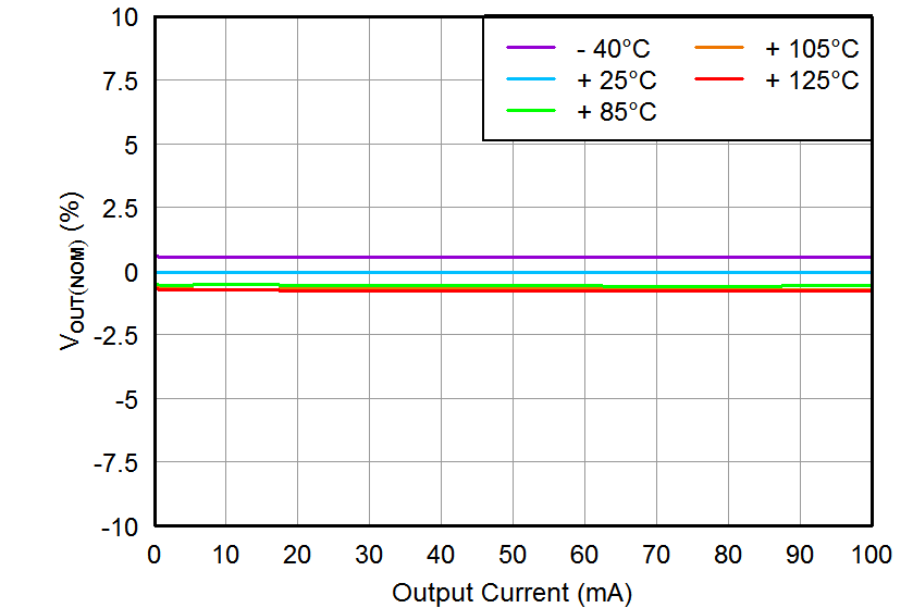
TPS7A16A-Q1 tc_vo-io_bvs171.png
Figure 7. Load Regulation
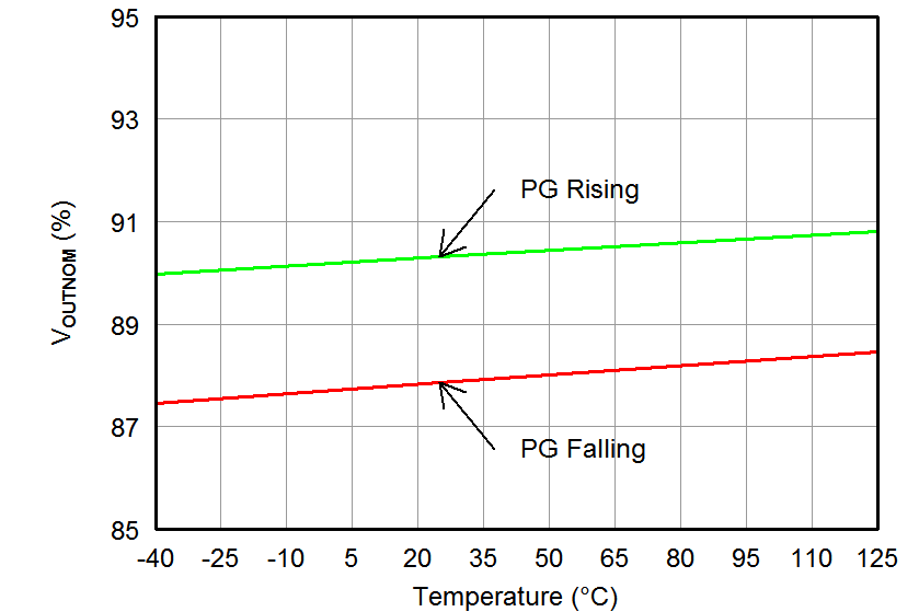
TPS7A16A-Q1 tc_vopg-temp_bvs171.png
Figure 9. Power-Good Threshold Voltage vs Temperature
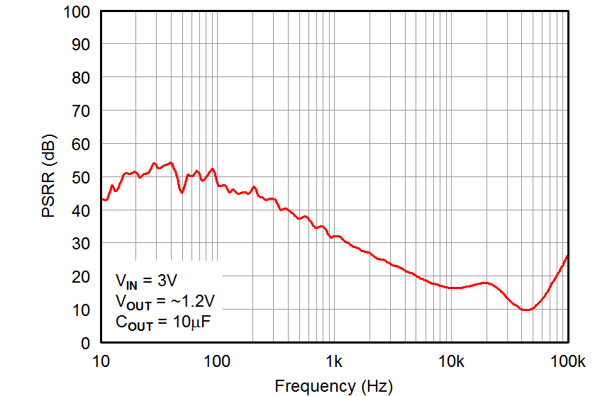
TPS7A16A-Q1 tc_psrr-freq_bvs171.png
Figure 11. Power-Supply Rejection Ratio vs Frequency
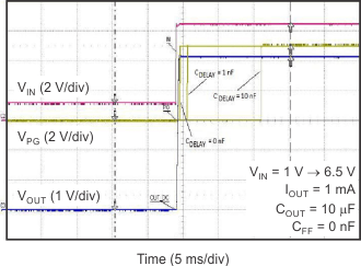
TPS7A16A-Q1 tc_pg-delay_bvs171.gif
Figure 13. Power-Good Delay
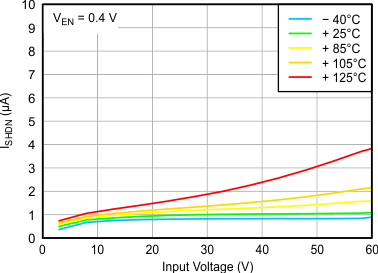
TPS7A16A-Q1 tc_ishdn-vin_SBVS188.gif
Figure 2. Shutdown Current vs Input Voltage
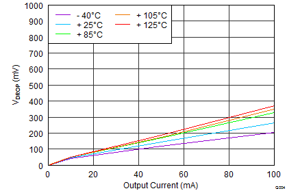
TPS7A16A-Q1 tc_vdo-io_bvs171.png
Figure 4. Dropout Voltage vs Output Current
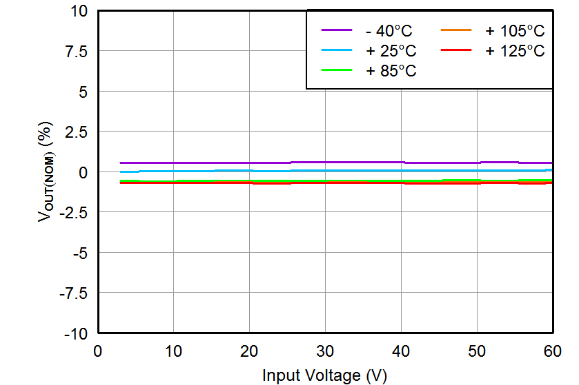
TPS7A16A-Q1 tc_vo-vin_bvs171.png
Figure 6. Line Regulation
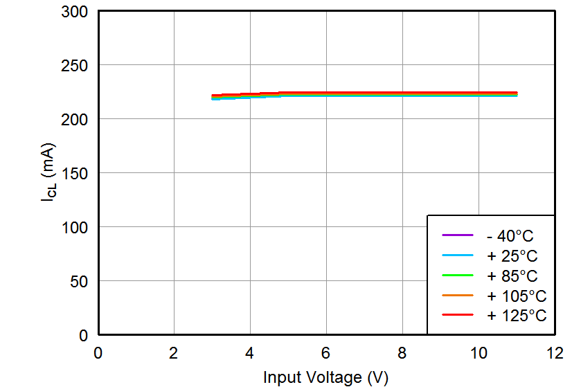
TPS7A16A-Q1 tc_ilim-vin_bvs171.png
Figure 8. Current Limit vs Input Voltage
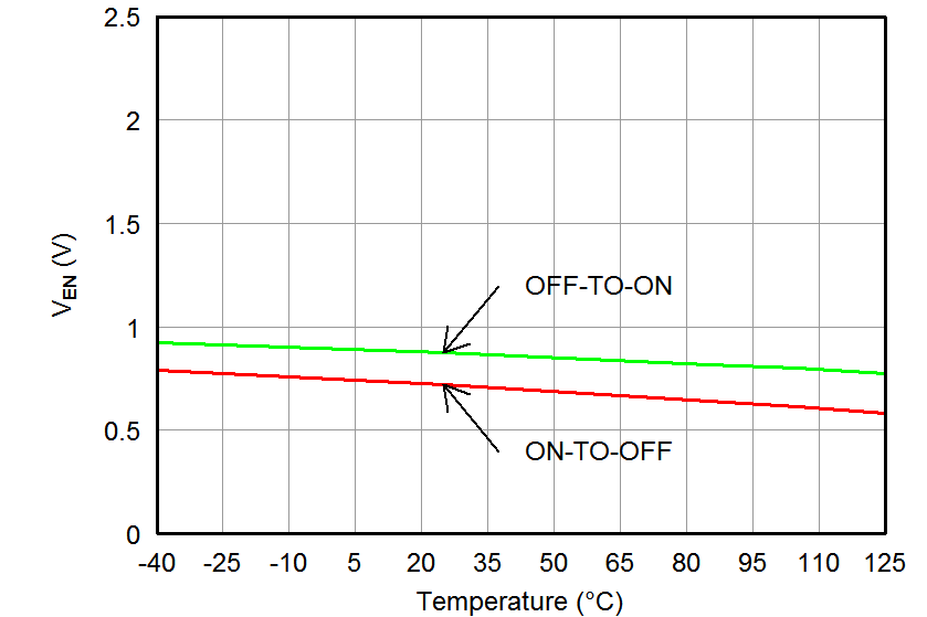
TPS7A16A-Q1 tc_ven-temp_bvs171.png
Figure 10. Enable Threshold Voltage vs Temperature
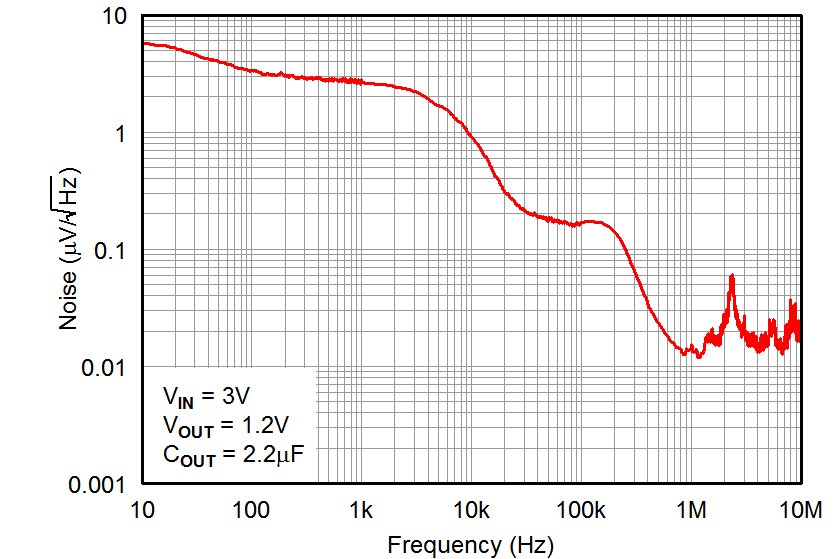
TPS7A16A-Q1 tc_vonoise-freq_bvs171.png
Figure 12. Output Spectral Noise Density