SBVS256A May 2016 – September 2016 TPS7A19
PRODUCTION DATA.
- 1 Features
- 2 Applications
- 3 Description
- 4 Revision History
- 5 Pin Configuration and Functions
- 6 Specifications
- 7 Detailed Description
- 8 Application and Implementation
- 9 Power Supply Recommendations
- 10Layout
- 11Device and Documentation Support
- 12Mechanical, Packaging, and Orderable Information
Package Options
Mechanical Data (Package|Pins)
- DRB|8
Thermal pad, mechanical data (Package|Pins)
- DRB|8
Orderable Information
1 Features
- Wide Input Voltage Range: 4 V to 40 V
- Adjustable Output Voltage: 1.5 V to 18 V
- Output Current: 450 mA
- Low Quiescent Current (IQ): 15 µA
- Low Dropout Voltage: 450 mV (max) at 400 mA
- Power Good with Programmable Delay
- Thermal Shutdown and Overcurrent Protection
- Stable with Ceramic Output Capacitors:
- 10 µF to 500 µF for VOUT ≥ 2.5 V
- 22 µF to 500 µF for VOUT < 2.5 V
- Operating Temperature: –40°C to +125°C
- Package: 3-mm × 3-mm SON-8
2 Applications
- Smart Grid Infrastructure and Metering
- Power Tools
- Motor Drives
- Access Control Systems
- Test and Measurement
3 Description
The TPS7A19 is a low-dropout linear regulator (LDO) with a wide input voltage (VIN) range up to 40 V, capable of sourcing high output current (IOUT) up to 450 mA. This voltage regulator is ideal for generating a low-voltage supply from wide input-voltage rails. Not only does the TPS7A19 supply a well-regulated voltage rail, but the device also withstands and maintains regulation during voltage transients by acting as a simple surge protection circuit.
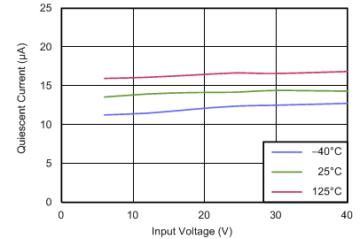
The TPS7A19 consumes only 15 µA of quiescent current (IQ) at light loads, thereby lowering the power consumption for always-on or battery-powered applications.
The TPS7A19 features integrated thermal shutdown and overcurrent protection. The TPS7A19 also offers a power good output (PG) with a programmable delay that indicates when the output voltage is in regulation. This feature is useful for power-rail sequencing functions.
This LDO is available in a small, 3-mm × 3-mm, thermally-enhanced, 8-pin SON package.
Device Information(1)
| PART NUMBER | PACKAGE | BODY SIZE (NOM) |
|---|---|---|
| TPS7A19 | SON (8) | 3.00 mm × 3.00 mm |
- For all available packages, see the package option addendum at the end of the data sheet.
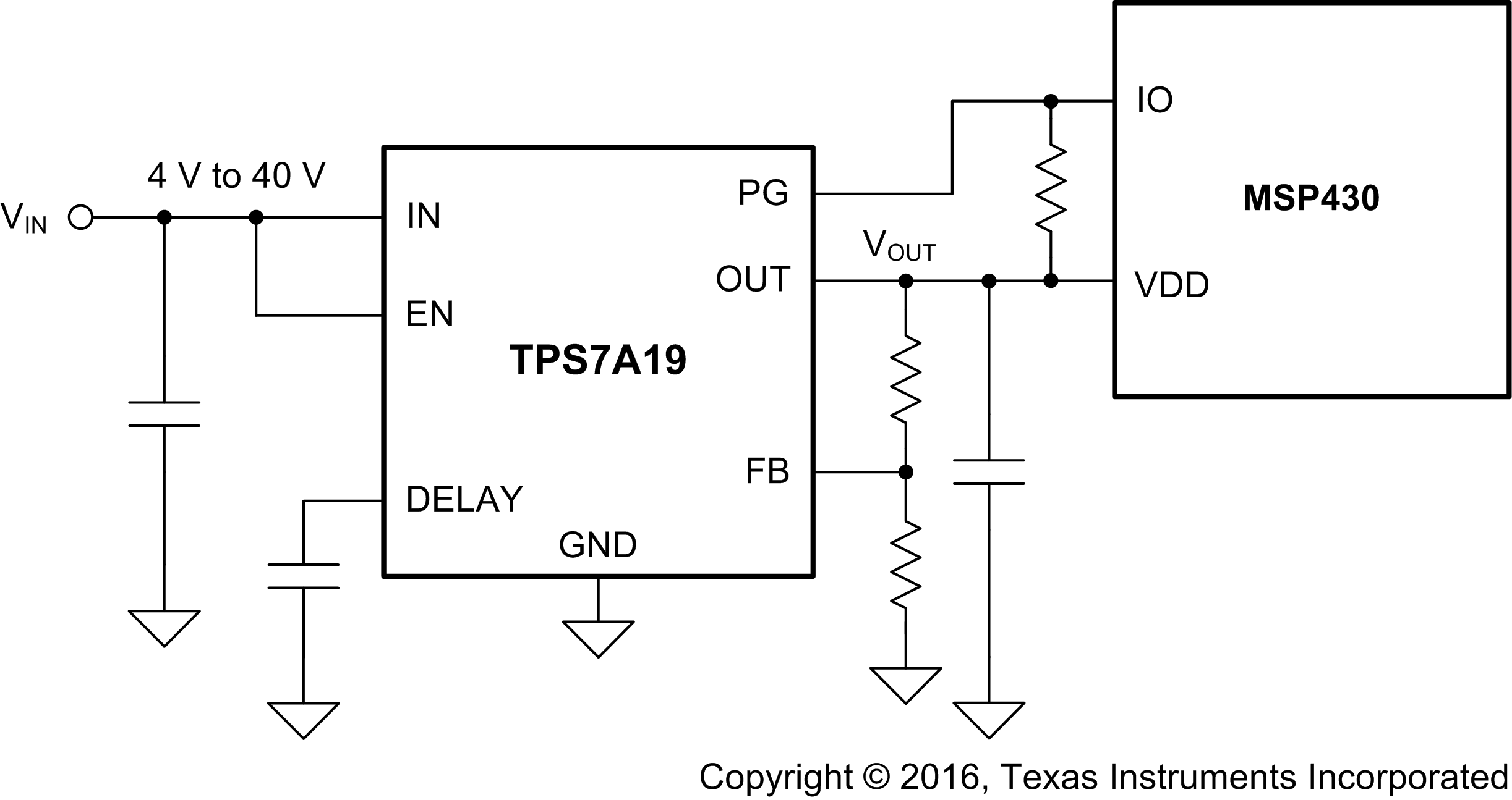
Typical Application Schematic

Quiescent Current vs Input Voltage
at VOUT = 1.5 V
