SBVS204F June 2012 – September 2014
PRODUCTION DATA.
- 1 Features
- 2 Applications
- 3 Description
- 4 Revision History
- 5 Pin Configuration and Functions
- 6 Specifications
- 7 Detailed Description
- 8 Application and Implementation
- 9 Power Supply Recommendations
- 10Layout
- 11Device and Documentation Support
- 12Mechanical, Packaging, and Orderable Information
Package Options
Mechanical Data (Package|Pins)
- RGW|20
Thermal pad, mechanical data (Package|Pins)
- RGW|20
Orderable Information
6 Specifications
6.1 Absolute Maximum Ratings
Over junction temperature range, unless otherwise noted.(1)| MIN | MAX | UNIT | |||
|---|---|---|---|---|---|
| Voltage(2) | IN pin to GND pin | –0.4 | +36 | V | |
| EN pin to GND pin | –0.4 | +36 | V | ||
| EN pin to IN pin | –36 | +0.4 | V | ||
| OUT pin to GND pin | –0.4 | +36 | V | ||
| NR pin to GND pin | –0.4 | +36 | V | ||
| SENSE/FB pin to GND pin | –0.4 | +36 | V | ||
| 0P1V pin to GND pin | –0.4 | +36 | V | ||
| 0P2V pin to GND pin | –0.4 | +36 | V | ||
| 0P4V pin to GND pin | –0.4 | +36 | V | ||
| 0P8V pin to GND pin | –0.4 | +36 | V | ||
| 1P6V pin to GND pin | –0.4 | +36 | V | ||
| 3P2V pin to GND pin | –0.4 | +36 | V | ||
| 6P4V1 pin to GND pin | –0.4 | +36 | V | ||
| 6P4V2 pin to GND pin | –0.4 | +36 | V | ||
| Current | Peak output | Internally limited | |||
| Temperature | Operating virtual junction, TJ | –40 | 125 | °C | |
(1) Stresses beyond those listed under Absolute Maximum Ratings may cause permanent damage to the device. These are stress ratings only, which do not imply functional operation of the device at these or any other conditions beyond those indicated under Recommended Operating Conditions. Exposure to absolute-maximum-rated conditions for extended periods may affect device reliability..
(2) All voltages are with respect to network ground terminal.
6.2 Handling Ratings
| MIN | MAX | UNIT | ||||
|---|---|---|---|---|---|---|
| Tstg | Storage temperature range | –65 | 150 | °C | ||
| V(ESD) | Electrostatic discharge | TPS7A4700 | Human body model (HBM), per ANSI/ESDA/JEDEC JS-001, all pins(1) | –1000 | 1000 | V |
| Charged device model (CDM), per JEDEC specification JESD22-C101, all pins(2) | –500 | 500 | ||||
| TPS7A4701 | Human body model (HBM), per ANSI/ESDA/JEDEC JS-001, all pins(1) | –2500 | 2500 | V | ||
| Charged device model (CDM), per JEDEC specification JESD22-C101, all pins(2) | –500 | 500 | ||||
(1) JEDEC document JEP155 states that 500-V HBM allows safe manufacturing with a standard ESD control process.
(2) JEDEC document JEP157 states that 250-V CDM allows safe manufacturing with a standard ESD control process.
6.3 Recommended Operating Conditions
over junction temperature range (unless otherwise noted)| MIN | NOM | MAX | UNIT | ||
|---|---|---|---|---|---|
| VI | 3.0 | 35.0 | V | ||
| VO | 1.4 | 34.0 | V | ||
| VEN | 0 | VIN | V | ||
| IO | 0 | 1.0 | A | ||
6.4 Thermal Information
| THERMAL METRIC(1) | TPS7A47xx | UNIT | |
|---|---|---|---|
| RGW | |||
| 20 PINS | |||
| RθJA | Junction-to-ambient thermal resistance | 32.5 | °C/W |
| RθJC(top) | Junction-to-case (top) thermal resistance | 27 | |
| RθJB | Junction-to-board thermal resistance | 11.9 | |
| ψJT | Junction-to-top characterization parameter | 0.3 | |
| ψJB | Junction-to-board characterization parameter | 11.9 | |
| RθJC(bot) | Junction-to-case (bottom) thermal resistance | 1.7 | |
(1) For more information about traditional and new thermal metrics, see the IC Package Thermal Metrics application report, SPRA953.
6.5 Electrical Characteristics
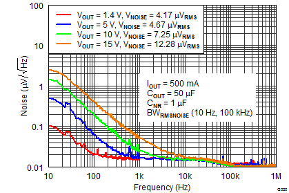
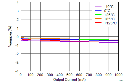
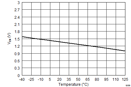
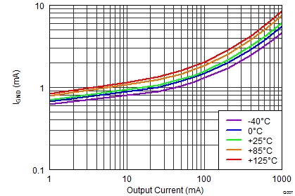
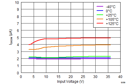
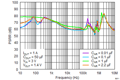
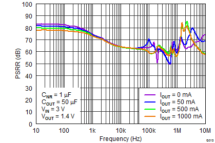
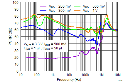
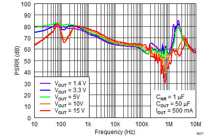
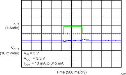
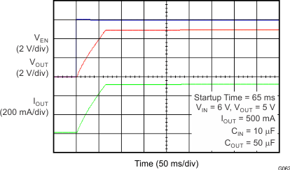
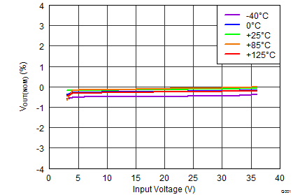
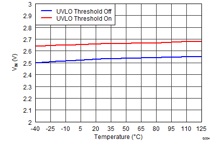
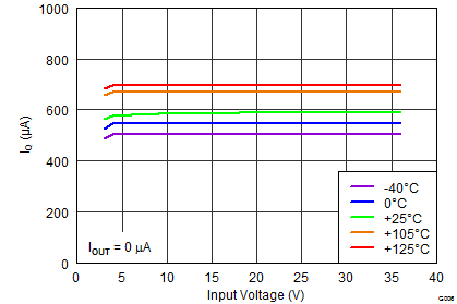
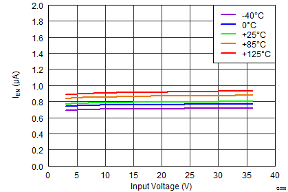
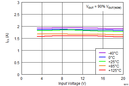
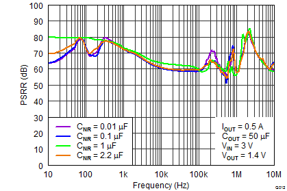
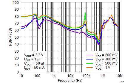
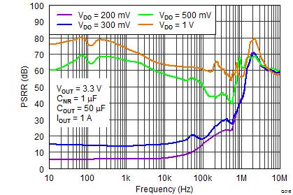
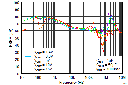
At –40°C ≤ TJ ≤ 125°C; VI = VO(nom) + 1.0 V or VI = 3.0 V (whichever is greater); VEN = VI; IO = 0 mA; CIN =10 µF; COUT = 10 µF; CNR = 10 nF; SENSE/FB tied to OUT; and 0P1V, 0P2V, 0P4V, 0P8V, 1P6V, 3P2V, 6P4V1, 6P4V2 pins OPEN, unless otherwise noted.6.6 Typical Characteristics
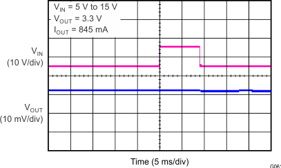
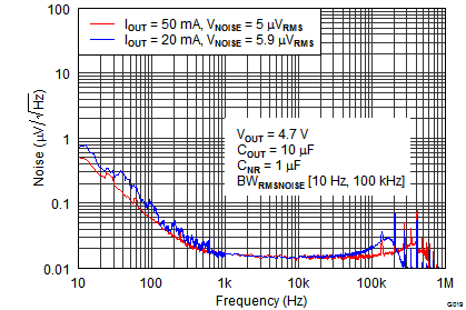
At –40°C ≤ TJ ≤ 125°C; VI = VO(nom) + 1.0 V or VI = 3.0 V (whichever is greater); VEN = VI; IO = 0 mA; CIN =10 µF; COUT = 10 µF; CNR = 1 µF; SENSE/FB tied to OUT; and 0P1V, 0P2V, 0P4V, 0P8V, 1P6V, 3P2V, 6P4V1, 6P4V2 pins OPEN, unless otherwise noted.