SBVS134F January 2012 – April 2017 TPS7A7001
PRODUCTION DATA.
- 1 Features
- 2 Applications
- 3 Description
- 4 Revision History
- 5 Pin Configuration and Functions
- 6 Specifications
- 7 Detailed Description
- 8 Application and Implementation
- 9 Power Supply Recommendations
- 10Layout
- 11Device and Documentation Support
- 12Mechanical, Packaging, and Orderable Information
Package Options
Mechanical Data (Package|Pins)
- DDA|8
Thermal pad, mechanical data (Package|Pins)
- DDA|8
Orderable Information
10 Layout
10.1 Layout Guidelines
10.1.1 Board Layout Recommendation to Improve PSRR and Noise Performance
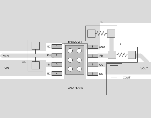
To improve ac measurements like PSRR, output noise, and transient response, use the board design shown in the layout example of Figure 8.
10.2 Layout Example
 Figure 8. Layout Example
10.3 Thermal Protection
Thermal protection disables the output when the junction temperature rises to approximately 160°C, allowing the device to cool. When the junction temperature cools to approximately 140°C, the output circuitry is re-enabled.
The internal protection circuitry of the TPS7A7001 is designed to protect against overload conditions. The protection circuitry is not intended to replace proper heat sinking. Continuously running the TPS7A7001 into thermal shutdown degrades device reliability.
10.4 Power Dissipation
Power dissipation (PD) of the device depends on the input voltage and load conditions and is calculated using Equation 2:

In order to minimize power dissipation and achieve greater efficiency, use the lowest possible input voltage necessary to achieve the required output voltage regulation
On the SO (DDA) package, the primary conduction path for heat is through the exposed pad to the printed circuit board (PCB). The pad can be connected to ground or left floating; however, attach the pad to an appropriate amount of copper PCB area to prevent the device from overheating. The maximum junction-to-ambient thermal resistance depends on the maximum ambient temperature, maximum device junction temperature, and power dissipation of the device, and is calculated using Equation 3:
