SBVS134F January 2012 – April 2017 TPS7A7001
PRODUCTION DATA.
- 1 Features
- 2 Applications
- 3 Description
- 4 Revision History
- 5 Pin Configuration and Functions
- 6 Specifications
- 7 Detailed Description
- 8 Application and Implementation
- 9 Power Supply Recommendations
- 10Layout
- 11Device and Documentation Support
- 12Mechanical, Packaging, and Orderable Information
Package Options
Mechanical Data (Package|Pins)
- DDA|8
Thermal pad, mechanical data (Package|Pins)
- DDA|8
Orderable Information
5 Pin Configuration and Functions
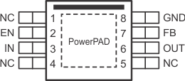
DDA Package
8-Pin SO PowerPAD
Top View

Pin Functions
| PIN | I/O | DESCRIPTION | |
|---|---|---|---|
| NAME | NO. | ||
| EN | 2 | I | Enable input. Pulling this pin below 0.5 V turns the regulator off. Connect to VIN if not being used. |
| FB | 7 | I | This pin is the output voltage feedback input through voltage dividers. See the Table 2 for more details. |
| GND | 8 | – | Ground pin |
| IN | 3 | I | Unregulated supply voltage pin. It is recommended to connect an input capacitor to this pin. |
| NC | 1, 4, 5 | – | Not internally connected. The NC pins are not connected to any electrical node. It is recommended to connect the NC pins to large-area planes. |
| OUT | 6 | O | Regulated output pin. A 4.7-μF or larger capacitor of any type is required for stability. |
| PowerPAD | TI strongly recommends connecting the thermal pad to a large-area ground plane. If an electrically floating, dedicated thermal plane is available, the thermal pad can also be connected to it. | ||