SLVSCK0A April 2014 – June 2014 TPS7A8101-Q1
PRODUCTION DATA.
- 1 Features
- 2 Applications
- 3 Description
- 4 Typical Application Circuit
- 5 Revision History
- 6 Pin Configuration and Functions
- 7 Specifications
- 8 Detailed Description
- 9 Application and Implementation
- 10Power Supply Recommendations
- 11Layout
- 12Device and Documentation Support
- 13Mechanical, Packaging, and Orderable Information
Package Options
Mechanical Data (Package|Pins)
- DRB|8
Thermal pad, mechanical data (Package|Pins)
- DRB|8
Orderable Information
6 Pin Configuration and Functions
8-Pin SON
DRB Package
(Top View)
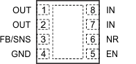
Pin Functions
| PIN | DESCRIPTION | |
|---|---|---|
| NAME | NO. | |
| EN | 5 | Driving this pin high turns on the regulator. Driving this pin low puts the regulator into shutdown mode. See to the Shutdown section for more details. The EN pin must not be left floating and can be connected to the IN pin if not used. |
| FB/SNS | 3 | This pin is the input to the error amplifier and is used to set the output voltage of the device. |
| GND | 4 | Ground |
| IN | 7 | Unregulated input supply |
| 8 | ||
| NR | 6 | Connect an external capacitor between this pin and ground to reduce output noise to very low levels. The capacitor also slows down the VO ramp (RC soft start). |
| OUT | 1 | Regulator output. A 4.7-μF or larger ceramic capacitor is required for stability. |
| 2 | ||
| Thermal Pad | — | The Thermal Pad should be connected to GND. |