SBVS318B July 2017 – January 2019 TPS7A92
PRODUCTION DATA.
- 1 Features
- 2 Applications
- 3 Description
- 4 Revision History
- 5 Pin Configuration and Functions
- 6 Specifications
-
7 Detailed Description
- 7.1 Overview
- 7.2 Functional Block Diagram
- 7.3 Feature Description
- 7.4 Device Functional Modes
- 8 Application and Implementation
- 9 Power Supply Recommendations
- 10Layout
- 11Device and Documentation Support
- 12Mechanical, Packaging, and Orderable Information
Package Options
Mechanical Data (Package|Pins)
- DSK|10
Thermal pad, mechanical data (Package|Pins)
- DSK|10
Orderable Information
7.3.6 Output Soft-Start Control
Soft-start refers to the ramp-up characteristic of the output voltage during LDO turn-on after the EN and UVLO thresholds are exceeded. The noise-reduction capacitor (CNR/SS) serves a dual purpose of both governing output noise reduction and programming the soft-start ramp during turn-on. Larger values for the noise-reduction capacitors decrease the noise but also result in a slower output turn-on ramp rate.
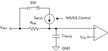
The TPS7A92 features an SS_CTRL pin. When the SS_CTRL pin is grounded, the charging current for the NR/SS pin is 6.2 µA (typ); when this pin is connected to IN, the charging current for the NR/SS pin is increased to 100 µA (typ). The higher current allows the use of a much larger noise-reduction capacitor and maintains a reasonable startup time. Figure 36 shows a simplified block diagram of the soft-start circuit. The switch SW is opened to turn off the INR/SS current source after VFB reaches approximately 97% of VREF. The final 3% of VNR/SS is charged through the noise reduction resistor (RNR), which creates an RC delay. RNR is approximately 280 kΩ and applications that require the highest accuracy when using a large value CNR/SS must take this RC delay into account.
If a noise-reduction capacitor is not used on the NR/SS pin, tying the SS_CTRL pin to the IN pin can result in output voltage overshoot of approximately 10%. This overshoot is minimized by either connecting the SS_CTRL pin to GND or using a capacitor on the NR/SS pin.
 Figure 36. Simplified Soft-Start Circuit