SBVS318B July 2017 – January 2019 TPS7A92
PRODUCTION DATA.
- 1 Features
- 2 Applications
- 3 Description
- 4 Revision History
- 5 Pin Configuration and Functions
- 6 Specifications
-
7 Detailed Description
- 7.1 Overview
- 7.2 Functional Block Diagram
- 7.3 Feature Description
- 7.4 Device Functional Modes
- 8 Application and Implementation
- 9 Power Supply Recommendations
- 10Layout
- 11Device and Documentation Support
- 12Mechanical, Packaging, and Orderable Information
Package Options
Mechanical Data (Package|Pins)
- DSK|10
Thermal pad, mechanical data (Package|Pins)
- DSK|10
Orderable Information
7.3.7 Power-Good Function
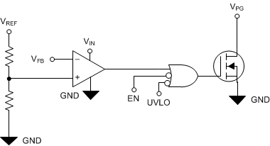
The power-good circuit monitors the voltage at the feedback pin to indicate the status of the output voltage. When the feedback pin voltage falls below the PG threshold voltage (VIT(PG)), the PG pin open-drain output engages and pulls the PG pin close to GND. When the feedback voltage exceeds the VIT(PG) threshold by an amount greater than VHYS(PG), the PG pin becomes high impedance. By connecting a pullup resistor to an external supply, any downstream device can receive power-good as a logic signal that can be used for sequencing. Make sure that the external pullup supply voltage results in a valid logic signal for the receiving device or devices. Using a pullup resistor from 10 kΩ to 100 kΩ is recommended. Using an external reset device such as the TPS3890 is also recommended in applications where high accuracy is needed or in applications where microprocessor induced resets are needed.
When using a feed-forward capacitor (CFF), the time constant for the LDO startup is increased whereas the power-good output time constant stays the same, possibly resulting in an invalid status of the power-good output. To avoid this issue and to receive a valid PG output, make sure that the time constant of both the LDO startup and the power-good output are matching, which can be done by adding a capacitor in parallel with the power-good pullup resistor. For more information, see the Pros and Cons of Using a Feedforward Capacitor with a Low-Dropout Regulator application report.
The state of PG is only valid when the device is operating above the minimum input voltage of the device and power good is asserted regardless of the output voltage state when the input voltage falls below the UVLO threshold minus the UVLO hysteresis. Figure 37 illustrates a simplified block diagram of the power-good circuit. When the input voltage falls below approximately 0.8 V, there is not enough gate drive voltage to keep the open-drain, power-good device turned on and the power-good output is pulled high. Connecting the power-good pullup resistor to the output voltage can help minimize this effect.
 Figure 37. Simplified PG Circuit