SLVSCE3A June   2014  – June 2014 TPS82740A , TPS82740B

PRODUCTION DATA.  

  1. Features
  2. Applications
  3. Description
    1.     Device Images
      1. 3.1 Typical Application
  4. Revision History
  5. Device Comparison Table
  6. Pin Configuration and Functions
    1.     Pin Functions
    2. Table 1. Output Voltage Setting TPS82740A
    3. Table 2. Output Voltage Setting TPS82740B
  7. Specifications
    1. 7.1 Absolute Maximum Ratings
    2. 7.2 ESD Ratings
    3. 7.3 Recommended Operating Conditions
    4. 7.4 Thermal Information
    5. 7.5 Electrical Characteristics
    6. 7.6 Typical Characteristics
  8. Parameter Measurement Information
  9. Detailed Description
    1. 9.1 Overview
    2. 9.2 Functional Block Diagram
    3. 9.3 Feature Description
      1. 9.3.1 DCS-Control
      2. 9.3.2 LOAD Switch
      3. 9.3.3 Output Voltage Selection (VSEL1, VSEL2, VSEL3)
      4. 9.3.4 Output Discharge Function (VOUT and LOAD)
      5. 9.3.5 Internal Current Limit
      6. 9.3.6 CTRL / DVS (Dynamic Voltage Scaling TPS62741)
    4. 9.4 Device Functional Modes
      1. 9.4.1 Enable / Shutdown
      2. 9.4.2 Soft Start
      3. 9.4.3 POWER GOOD OUTPUT (PG)
      4. 9.4.4 Automatic Transition into 100% Mode
  10. 10Application and Implementation
    1. 10.1 Application Information
    2. 10.2 Typical Application
      1. 10.2.1 Design Requirements
      2. 10.2.2 Detailed Design Procedure
        1. 10.2.2.1 Input Capacitor Selection
          1. 10.2.2.1.1 Input Buffer Capacitor Selection
        2. 10.2.2.2 Output Capacitor Selection
      3. 10.2.3 Application Curves
  11. 11Power Supply Recommendations
  12. 12Layout
    1. 12.1 Layout Guidelines
    2. 12.2 Layout Example
    3. 12.3 Surface Mount Information
  13. 13Device and Documentation Support
    1. 13.1 Documentation Support
      1. 13.1.1 Related Links
    2. 13.2 Trademarks
    3. 13.3 Electrostatic Discharge Caution
    4. 13.4 Glossary
  14. 14Mechanical, Packaging, and Orderable Information
    1. 14.1 Tape and Reel Information

Package Options

Refer to the PDF data sheet for device specific package drawings

Mechanical Data (Package|Pins)
  • SIP|9
Thermal pad, mechanical data (Package|Pins)
Orderable Information

Automatic Transition into 100% Mode

Once the input voltage comes close to the output voltage, the TPS82740 stops switching and enters 100% duty cycle operation. It connects the output VOUT via the inductor and the internal high side MOSFET switch to the input VIN, once the input voltage VIN falls below the 100% mode enter threshold, VTH_100-. In 100% mode switching stops eliminating output voltage ripple. Because the output is connected to the input, the output voltage tracks the input voltage minus the voltage drop across the internal high side switch and the inductor caused by the output current. Once the input voltage increases and trips the 100% mode exit threshold, VTH_100+ , the TPS82740 turns on and starts switching again. See Figure 40, Figure 18, Figure 19 and Figure 20.
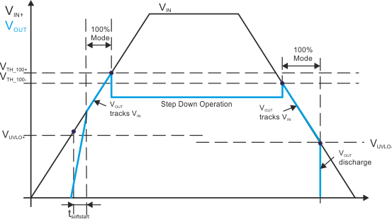
TPS82740A TPS82740B TPS82740_status_diagram_auto100mode_pg.gifFigure 40. Automatic Transition into 100% Mode