SLVSCE3A June   2014  – June 2014 TPS82740A , TPS82740B

PRODUCTION DATA.  

  1. Features
  2. Applications
  3. Description
    1.     Device Images
      1. 3.1 Typical Application
  4. Revision History
  5. Device Comparison Table
  6. Pin Configuration and Functions
    1.     Pin Functions
    2. Table 1. Output Voltage Setting TPS82740A
    3. Table 2. Output Voltage Setting TPS82740B
  7. Specifications
    1. 7.1 Absolute Maximum Ratings
    2. 7.2 ESD Ratings
    3. 7.3 Recommended Operating Conditions
    4. 7.4 Thermal Information
    5. 7.5 Electrical Characteristics
    6. 7.6 Typical Characteristics
  8. Parameter Measurement Information
  9. Detailed Description
    1. 9.1 Overview
    2. 9.2 Functional Block Diagram
    3. 9.3 Feature Description
      1. 9.3.1 DCS-Control
      2. 9.3.2 LOAD Switch
      3. 9.3.3 Output Voltage Selection (VSEL1, VSEL2, VSEL3)
      4. 9.3.4 Output Discharge Function (VOUT and LOAD)
      5. 9.3.5 Internal Current Limit
      6. 9.3.6 CTRL / DVS (Dynamic Voltage Scaling TPS62741)
    4. 9.4 Device Functional Modes
      1. 9.4.1 Enable / Shutdown
      2. 9.4.2 Soft Start
      3. 9.4.3 POWER GOOD OUTPUT (PG)
      4. 9.4.4 Automatic Transition into 100% Mode
  10. 10Application and Implementation
    1. 10.1 Application Information
    2. 10.2 Typical Application
      1. 10.2.1 Design Requirements
      2. 10.2.2 Detailed Design Procedure
        1. 10.2.2.1 Input Capacitor Selection
          1. 10.2.2.1.1 Input Buffer Capacitor Selection
        2. 10.2.2.2 Output Capacitor Selection
      3. 10.2.3 Application Curves
  11. 11Power Supply Recommendations
  12. 12Layout
    1. 12.1 Layout Guidelines
    2. 12.2 Layout Example
    3. 12.3 Surface Mount Information
  13. 13Device and Documentation Support
    1. 13.1 Documentation Support
      1. 13.1.1 Related Links
    2. 13.2 Trademarks
    3. 13.3 Electrostatic Discharge Caution
    4. 13.4 Glossary
  14. 14Mechanical, Packaging, and Orderable Information
    1. 14.1 Tape and Reel Information

Package Options

Refer to the PDF data sheet for device specific package drawings

Mechanical Data (Package|Pins)
  • SIP|9
Thermal pad, mechanical data (Package|Pins)
Orderable Information

Typical Characteristics

TABLE OF GRAPHS FIGURE
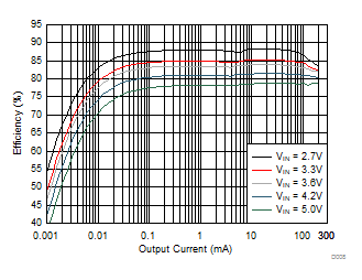
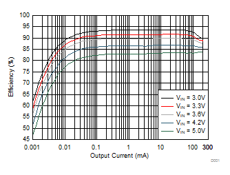
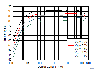
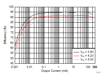
η Efficiency vs Output Current Figure 3, Figure 4, Figure 5, Figure 6
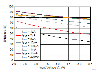
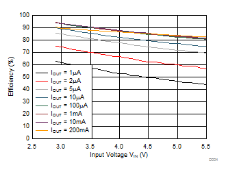
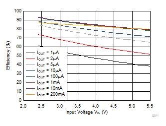
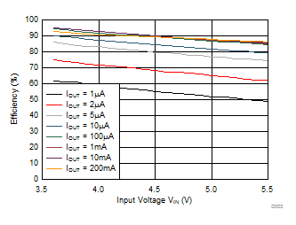
η Efficiency vs Input Voltage Figure 7, Figure 8, Figure 9, Figure 10
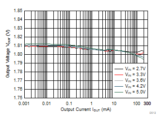
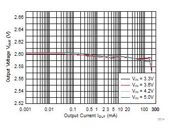
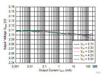
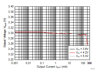
VOUT Output voltage vs Output curent Figure 11, Figure 12, Figure 13, Figure 14
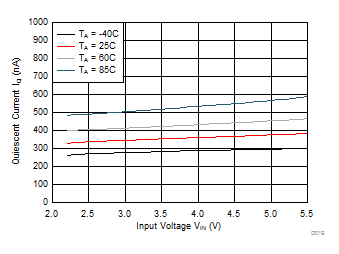
IQ Operating quiescent current vs Input voltage Figure 1
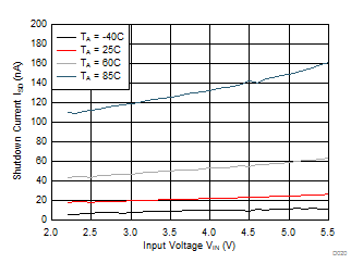
ISD Shutdown current vs Input voltage Figure 2
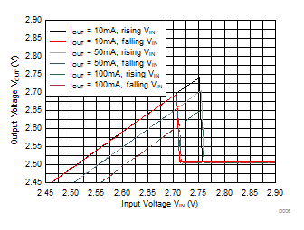
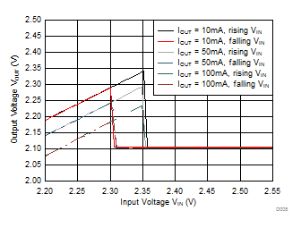
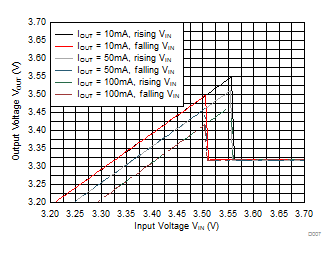
Automatic Transition into 100% Mode Figure 18, Figure 19, Figure 20
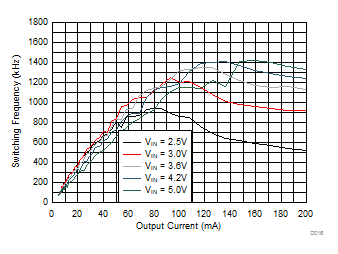
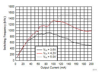
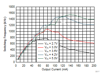
FSW Switching frequency vs Output current Figure 15, Figure 16, Figure 17
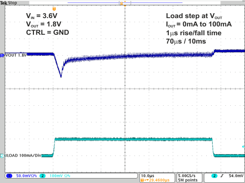
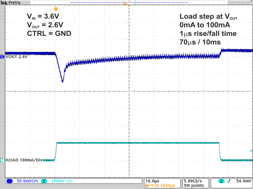
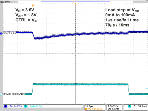
Line and Load Transient Performance Figure 21, Figure 22, Figure 23, Figure 24, Figure 25, Figure 26, Figure 27, Figure 28, Figure 29, Figure 30
AC load regulation performance Figure 31, Figure 32
LOAD LOAD Output Behavior Figure 33, Figure 34, Figure 35
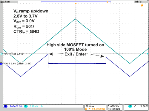
Input Voltage Ramp up / down Figure 36, Figure 37, Figure 38, Figure 39
TPS82740A TPS82740B D019_SLVSCE3_TPS82740.gif
EN = VIN CTRL = GND
Device not switching
Figure 1. TPS82740 Quiescent Current IQ
TPS82740A TPS82740B D008_SLVSCE3_TPS82740.gif
CTRL = GND
Figure 3. TPS82740A Efficiency VOUT = 1.8V
TPS82740A TPS82740B D001_SLVSCE3_TPS82740.gif
CTRL = GND
Figure 5. TPS82740B Efficiency VOUT = 2.6V
TPS82740A TPS82740B D010_SLVSCE3_TPS82740.gif
CTRL = GND
Figure 7. TPS82740A Efficiency VOUT = 1.8V
TPS82740A TPS82740B D004_SLVSCE3_TPS82740.gif
CTRL = GND
Figure 9. TPS82740B Efficiency VOUT = 2.6V
TPS82740A TPS82740B D012_SLVSCE3_TPS82740.gif
CTRL = GND
Figure 11. TPS82740A Output voltage VOUT = 1.8V
TPS82740A TPS82740B D014_SLVSCE3_TPS82740.gif
CTRL = GND
Figure 13. TPS82740B Output voltage VOUT = 2.6V
TPS82740A TPS82740B D016_SLVSCE3_TPS82740.gif
Figure 15. TPS82740A Switching frequency VOUT = 1.8V
TPS82740A TPS82740B D018_SLVSCE3_TPS82740.gif
Figure 17. TPS82740B switching frequency VOUT = 3.0V
TPS82740A TPS82740B D006_SLVSCE3_TPS82740.gif
Figure 19. TPS82740A 100% Mode Transition VOUT = 2.5V
TPS82740A TPS82740B 1- 50uA to 10mA Vout 1.8V.gif
Figure 21. TPS82740A Load Transient Response VOUT = 1.8V
TPS82740A TPS82740B 3- 50uA to 10mA Vout 2.6V.gif
Figure 23. TPS82740B Load Transient Response VOUT = 2.6V
TPS82740A TPS82740B 5 - 0mA to 100mA Vout 1.8V.gif
Figure 25. TPS82740A Load Transient Response VOUT = 1.8V
TPS82740A TPS82740B 7- 0mA to 100mA Vout 2.6V.gif
Figure 27. TPS82740B Load Transient Response VOUT = 2.6V
TPS82740A TPS82740B 9- line 10mA 2V1.gif
Figure 29. TPS82740A Line Transient Response
IOUT = 10mA
TPS82740A TPS82740B 11- 50uA to 200mA sweep Vout 1.8V.gif
Figure 31. TPS82740A AC Load Sweep VOUT = 1.8V
TPS82740A TPS82740B 13- Loadstep at LOAD 0 to 50mA 1.8V.gif
Figure 33. TPS82740A Load Step at LOAD Output
TPS82740A TPS82740B 15- Load output on off 2.6V.gif
Figure 35. TPS82740B Load Output ON / OFF
TPS82740A TPS82740B 21- input voltage ramp 2.6V.gif
Figure 37. TPS82740B Input Voltage Ramp Up / Down
TPS82740A TPS82740B 23- Enter - Exit 100 pro mode.gif
Figure 39. TPS82740B Enter / Exit 100% Mode Operation
TPS82740A TPS82740B D020_SLVSCE3_TPS82740.gif
EN = GND
Figure 2. TPS82740 Shutdown current ISD
TPS82740A TPS82740B D009_SLVSCE3_TPS82740.gif
CTRL = GND
Figure 4. TPS82740A Efficiency VOUT = 2.1V
TPS82740A TPS82740B D002_SLVSCE3_TPS82740.gif
CTRL = GND
Figure 6. TPS82740B Efficiency VOUT = 3.3V
TPS82740A TPS82740B D011_SLVSCE3_TPS82740.gif
CTRL = GND
Figure 8. TPS82740A Efficiency VOUT = 2.1V
TPS82740A TPS82740B D003_SLVSCE3_TPS82740.gif
CTRL = GND
Figure 10. TPS82740B Efficiency VOUT = 3.3V
TPS82740A TPS82740B D013_SLVSCE3_TPS82740.gif
Figure 12. TPS82740A Output voltage VOUT = 2.1V
TPS82740A TPS82740B D015_SLVSCE3_TPS82740.gif
CTRL = GND
Figure 14. TPS82740B Output voltage VOUT = 3.3V
TPS82740A TPS82740B D017_SLVSCE3_TPS82740.gif
Figure 16. TPS82740A Switching frequency VOUT = 2.1V
TPS82740A TPS82740B D005_SLVSCE3_TPS82740.gif
Figure 18. TPS82740A 100% Mode Transition VOUT = 2.1V
TPS82740A TPS82740B D007_SLVSCE3_TPS82740.gif
Figure 20. TPS82740B 100% Mode Transition VOUT = 3.3V
TPS82740A TPS82740B 2- 0.5mA to 150mA Vout 1.8V CTRL=VIN.gif
Figure 22. TPS82740A Load Transient Response VOUT = 1.8V
TPS82740A TPS82740B 4- 0.5mA to 150mA Vout 2.6V CTRL=VIN.gif
Figure 24. TPS82740B Load Transient Response VOUT = 2.6V
TPS82740A TPS82740B 6- 0mA to 100mA Vout 1.8V CTRL H.gif
Figure 26. TPS82740A Load Transient Response VOUT = 1.8V
TPS82740A TPS82740B 8- 0mA to 100mA Vout 2.6V CTRL H.gif
Figure 28. TPS82740B Load Transient response VOUT = 2.6V
TPS82740A TPS82740B 10- line 100mA 2V1.gif
Figure 30. TPS82740A Line Transient Response
IOUT = 100mA
TPS82740A TPS82740B 12- 50uA to 200mA sweep Vout 2.6V.gif
Figure 32. TPS82740B AC Load Sweep VOUT = 2.6V
TPS82740A TPS82740B 14- Loadstep at LOAD 0 to 50mA 2.6V.gif
Figure 34. TPS82740B Load Step at LOAD Output
TPS82740A TPS82740B 20- input voltage ramp 1.8V.gif
Figure 36. TPS82740A Input Voltage Ramp Up / Down
TPS82740A TPS82740B 22- input voltage ramp 3.3V.gif
Figure 38. TPS82740B Input Voltage Ramp Up / Down