SLIS178B October   2017  – January 2018 TPS92830-Q1

PRODUCTION DATA.  

  1. Features
  2. Applications
  3. Description
    1.     Simplified Schematic
  4. Revision History
  5. Description (Continued)
  6. Pin Configuration and Functions
    1.     Pin Functions
  7. Specifications
    1. 7.1 Absolute Maximum Ratings
    2. 7.2 ESD Ratings
    3. 7.3 Recommended Operating Conditions
    4. 7.4 Thermal Information
    5. 7.5 Electrical Characteristics
    6. 7.6 Timing Requirements
    7. 7.7 Typical Characteristics
  8. Detailed Description
    1. 8.1 Overview
    2. 8.2 Functional Block Diagram
    3. 8.3 Feature Description
      1. 8.3.1 Device Bias
        1. 8.3.1.1 Power-On-Reset (POR)
        2. 8.3.1.2 Current Reference (IREF)
        3. 8.3.1.3 Low-Current Fault Mode
      2. 8.3.2 Charge Pump
        1. 8.3.2.1 Charge Pump Architecture
      3. 8.3.3 Constant-Current Driving
        1. 8.3.3.1 High-Side Current Sense
        2. 8.3.3.2 High-Side Current Driving
        3. 8.3.3.3 Gate Overdrive Voltage Protection
        4. 8.3.3.4 High-Precision Current Regulation
        5. 8.3.3.5 Parallel MOSFET Driving
      4. 8.3.4 PWM Dimming
        1. 8.3.4.1 Supply Dimming
        2. 8.3.4.2 PWM Dimming by Input
        3. 8.3.4.3 Internal Precision PWM Generator
        4. 8.3.4.4 Full Duty-Cycle Switch
      5. 8.3.5 Analog Dimming
        1. 8.3.5.1 Analog Dimming Topology
        2. 8.3.5.2 Internal High-Precision Pullup Current Source
      6. 8.3.6 Output Current Derating
        1. 8.3.6.1 Output-Current Derating Topology
      7. 8.3.7 Diagnostics and Fault
        1. 8.3.7.1 LED Short-to-GND Detection
        2. 8.3.7.2 LED Short-to-GND Auto Retry
        3. 8.3.7.3 LED Open-Circuit Detection
        4. 8.3.7.4 LED Open-Circuit Auto Retry
        5. 8.3.7.5 Dropout-Mode Diagnostics
        6. 8.3.7.6 Overtemperature Protection
        7. 8.3.7.7 FAULT Bus Output With One-Fails–All-Fail
        8. 8.3.7.8 Fault Table
    4. 8.4 Device Functional Modes
      1. 8.4.1 Undervoltage Lockout, V(IN) < V(UVLO)
      2. 8.4.2 Normal Operation (V(IN) ≥ 4.5 V, V(IN) > V(LED) + 0.5 V)
      3. 8.4.3 Low-Voltage Dropout
      4. 8.4.4 Fault Mode (Fault Is Detected)
  9. Application and Implementation
    1. 9.1 Application Information
    2. 9.2 Typical Applications
      1. 9.2.1 Typical Application for Automotive Exterior Lighting With One-Fails–All-Fail
        1. 9.2.1.1 Design Requirements
        2. 9.2.1.2 Detailed Design Procedure
        3. 9.2.1.3 Application Curves
      2. 9.2.2 High-Precision Dual-Brightness PWM Generation
        1. 9.2.2.1 Dual-Brightness Application
        2. 9.2.2.2 Design Requirements
        3. 9.2.2.3 Detailed Design Procedure
        4. 9.2.2.4 Application Curve
      3. 9.2.3 Driving High-Current LEDs With Parallel MOSFETs
        1. 9.2.3.1 Application Curves
  10. 10Layout
    1. 10.1 Layout Guidelines
    2. 10.2 Layout Example
  11. 11Device and Documentation Support
    1. 11.1 Receiving Notification of Documentation Updates
    2. 11.2 Community Resources
    3. 11.3 Trademarks
    4. 11.4 Electrostatic Discharge Caution
    5. 11.5 Glossary
  12. 12Mechanical, Packaging, and Orderable Information

Package Options

Mechanical Data (Package|Pins)
Thermal pad, mechanical data (Package|Pins)
Orderable Information

Typical Characteristics

TA = 25 ºC unless otherwise noted
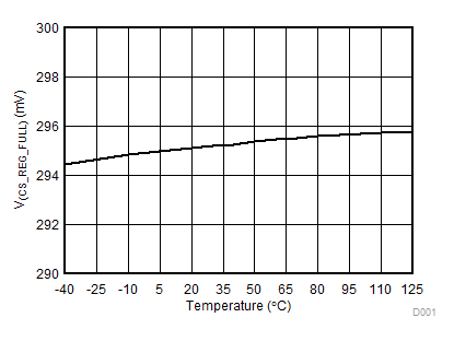
TPS92830-Q1 D001_CSREG_TEMP_SLDS233.gif
V(IN) = 14 V V(ICTRL) = 1.8 V
Figure 2. Full-Range Current-Sense Voltage vs Ambient Temperature
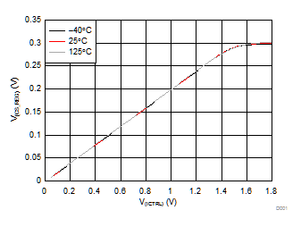
TPS92830-Q1 D001_SLIS178.gif
V(IN) = 14 V
Figure 4. Current-Sense Voltage vs ICTRL Input Voltage
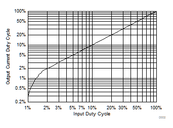
TPS92830-Q1 D002_SLIS178.gif
V(IN) = 14 V f(PWM)= 200 Hz V(ICTRL) = 1.8 V
Figure 6. Duty Cycle of PWM Dimming-Current Output vs PWM Input Duty Cycle
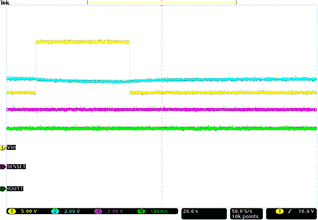
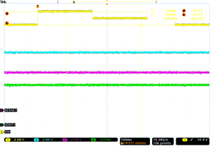
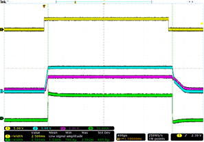
TPS92830-Q1 Typ_App_1_PWM_Pulse_SLIS178.gif
Ch. 1 = PWM1 Ch. 2 = G1 Ch. 3 = SENSE1
Ch. 4 = I(OUT1) V(IN) = 14 V
Figure 8. PWM Dimming
TPS92830-Q1 Typ_App_4_UnderVoltage_SLIS178.gif
Ch. 1 = V(IN) Ch. 2 = G1 Ch. 3 = SENSE1
Ch. 4 = I(OUT1)
Figure 10. Undervoltage
TPS92830-Q1 Typ_App_6_Jump_Start_SLIS178.gif
Ch. 1 = V(IN) Ch. 2 = G1 Ch. 3 = SENSE1
Ch. 4 = I(OUT1)
Figure 12. Jump Start
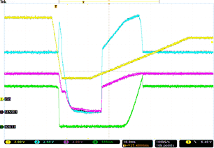
TPS92830-Q1 Typ_App_3_ColdCrank_SLIS178.gif
Ch. 1 = V(IN) Ch. 2 = G1 Ch. 3 = SENSE1
Ch. 4 = I(OUT1)
Figure 14. Fast Power Down and Slow Power Up
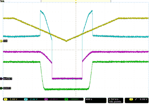
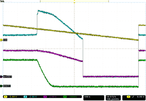
TPS92830-Q1 Typ_App_8_Slow_Ramp_Down_Slow_Ramp_Up_SLIS178.gif
Ch. 1 = V(IN) Ch. 2 = G1 Ch. 3 = SENSE1
Ch. 4 = I(OUT1)
Figure 16. Slow Decrease and Slow Increase of Supply Voltage
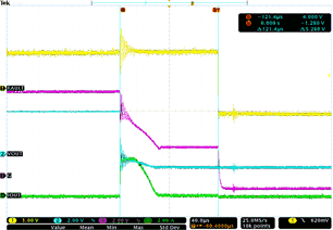
TPS92830-Q1 Typ_App_10_Short_To_Ground_SLIS178.gif
Ch. 1 = FAULT Ch. 2 = SENSE1 Ch. 3 = G1
Ch. 4 = I(OUT1) LED short-to-ground on SENSE1
Figure 18. LED Hard Short Protection and One-Fails–All-Fail
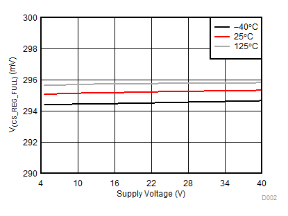
TPS92830-Q1 D002_CSREG_SUPPLY_SLDS233.gif
V(ICTRL) = 1.8 V
Figure 3. Full-Range Current-Sense Voltage vs Supply Voltage
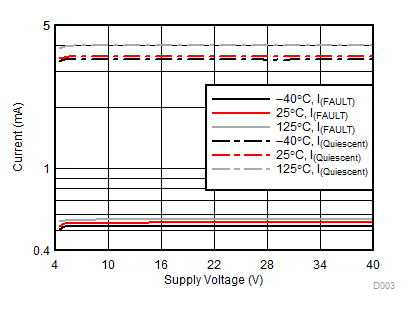
TPS92830-Q1 D003_IQ_SUPPLY_SLDS233.gif
Figure 5. Device Current vs Supply Voltage
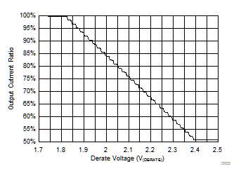
TPS92830-Q1 D003_SLIS178.gif
V(IN) = 14 V
Figure 7. Current-Derating Profile; Output-Current Ratio vs DERATE Voltage
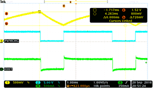
TPS92830-Q1 Typ_App_2_PWM_Generator_SLIS178.gif
Ch. 1 = PWMCHG Ch. 2 = PWMOUT Ch. 4 = I(OUT1)
V(IN) = 14 V
Figure 9. PWM Generator
TPS92830-Q1 Typ_App_5_Transient_Voltage_SLIS178.gif
Ch. 1 = V(IN) Ch. 2 = G1 Ch. 3 = SENSE1
Ch. 4 = I(OUT1)
Figure 11. Transient Overvoltage
TPS92830-Q1 Typ_App_6_Superimposed_15Hz_SLIS178.gif
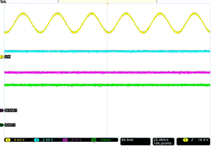
Ch. 1 = V(IN) Ch. 2 = G1 Ch. 3 = SENSE1
Ch. 4 = I(OUT1) ƒ = 15 Hz
Figure 13. Superimposed Alternating Voltage
TPS92830-Q1 Typ_App_7_Slow_Ramp_Down_SLIS178.gif
Ch. 1 = V(IN) Ch. 2 = G1 Ch. 3 = SENSE1
Ch. 4 = I(OUT1)
Figure 15. Slow Decrease, Quick Increase of Supply Voltage
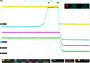
TPS92830-Q1 Typ_App_9_Open_Circuit_SLIS178.gif
Ch. 1 = FAULT Ch. 2 = SENSE1 Ch. 3 = SENSE2
Ch. 4 = SENSE3 LED open-circuit on SENSE1
Figure 17. LED Open-Circuit Protection and One-Fails–All-Fail
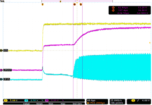
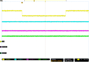
TPS92830-Q1 Typ_App_11_Start_Delay_SLIS178.gif
Ch. 1 = V(IN) Ch. 2 = CP1N Ch. 3 = CPOUT
Figure 19. Device Start-Up Delay