SLLS850D January 2008 – March 2017 TRS3253E
PRODUCTION DATA.
- 1 Features
- 2 Applications
- 3 Description
- 4 Revision History
- 5 Pin Configuration and Functions
-
6 Specifications
- 6.1 Absolute Maximum Ratings
- 6.2 ESD Ratings
- 6.3 Recommended Operating Conditions
- 6.4 Thermal Information
- 6.5 Electrical Characteristics—Power
- 6.6 Electrical Characteristics—Driver
- 6.7 Electrical Characteristics—Receiver
- 6.8 Electrical Characteristics—Status
- 6.9 Switching Characteristics—Driver
- 6.10 Switching Characteristics—Receiver
- 6.11 Switching Characteristics—Power and Status
- 6.12 Typical Characteristics
- 7 Parameter Measurement Information
- 8 Detailed Description
- 9 Application and Implementation
- 10Power Supply Recommendations
- 11Layout
- 12Device and Documentation Support
- 13Mechanical, Packaging, and Orderable Information
Package Options
Mechanical Data (Package|Pins)
- RSM|32
Thermal pad, mechanical data (Package|Pins)
- RSM|32
Orderable Information
9 Application and Implementation
NOTE
Information in the following applications sections is not part of the TI component specification, and TI does not warrant its accuracy or completeness. TI’s customers are responsible for determining suitability of components for their purposes. Customers should validate and test their design implementation to confirm system functionality.
9.1 Application Information
This device can be used in any application where an RS232 line driver or receiver is required. One benefit of this device is its ESD protection, which helps protect other components on the board when the RS232 lines are tied to a physical connector.
9.2 Typical Application
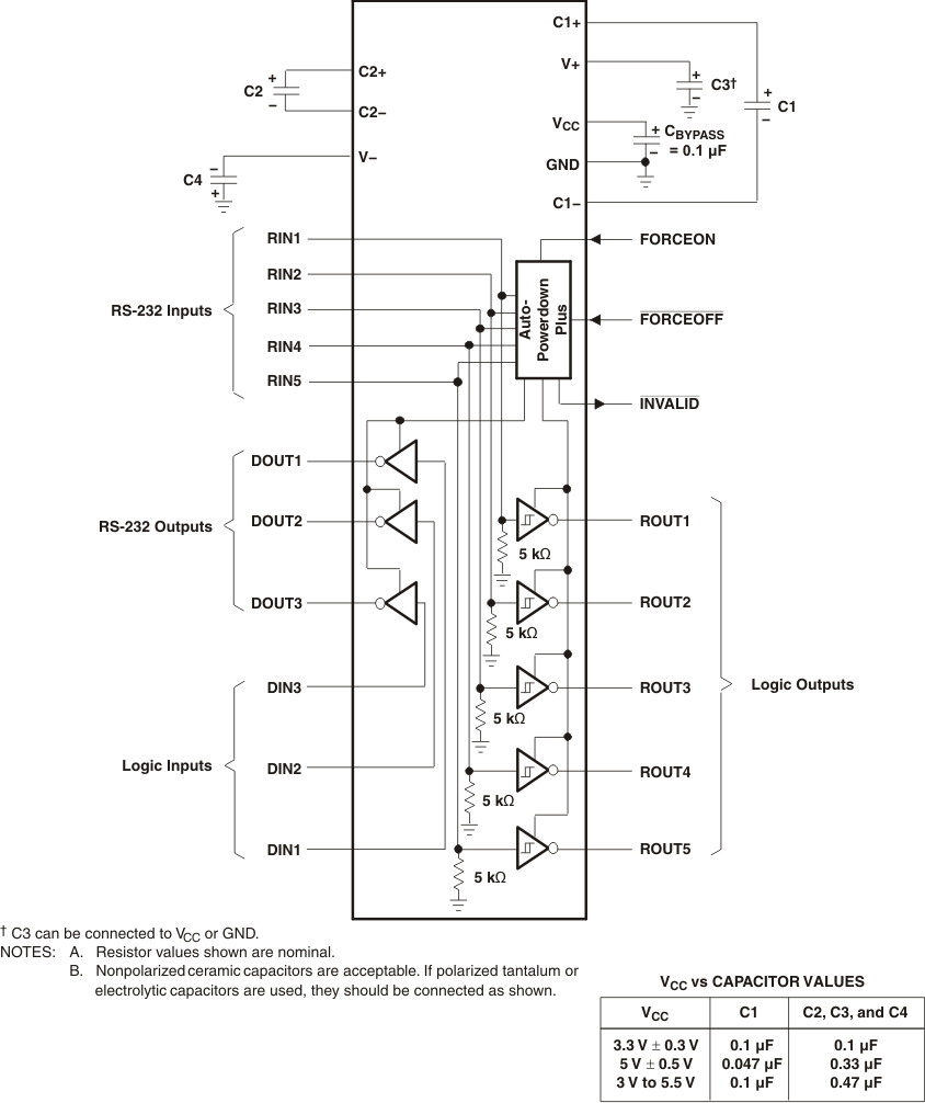
ROUT and DIN connect to UART or general purpose logic lines. FORCEON and FORCEOFF may be connected general purpose logic lines or tied to ground or VL. INVALID may be connected to a general purpose logic line or left unconnected. RIN and DOUT lines connect to a RS232 connector or cable. DIN, FORCEON, and FORCEOFF inputs must not be left unconnected. For proper operation, add capacitors as shown in Figure 8.
 Figure 8. Typical Operating Circuit and Capacitor Values
9.2.1 Design Requirements
- Recommended VCC is 3.3 V or 5 V. 3 V to 5.5 V is also possible
- Maximum recommended bit rate is 1000 kbps
- Use capacitors as shown in Figure 8
9.2.2 Detailed Design Procedure
- All DIN, FORCEOFF, and FORCEON inputs must be connected to valid low or high logic levels.
- Select capacitor values based on VCC level for best performance.
9.2.3 Application Curve
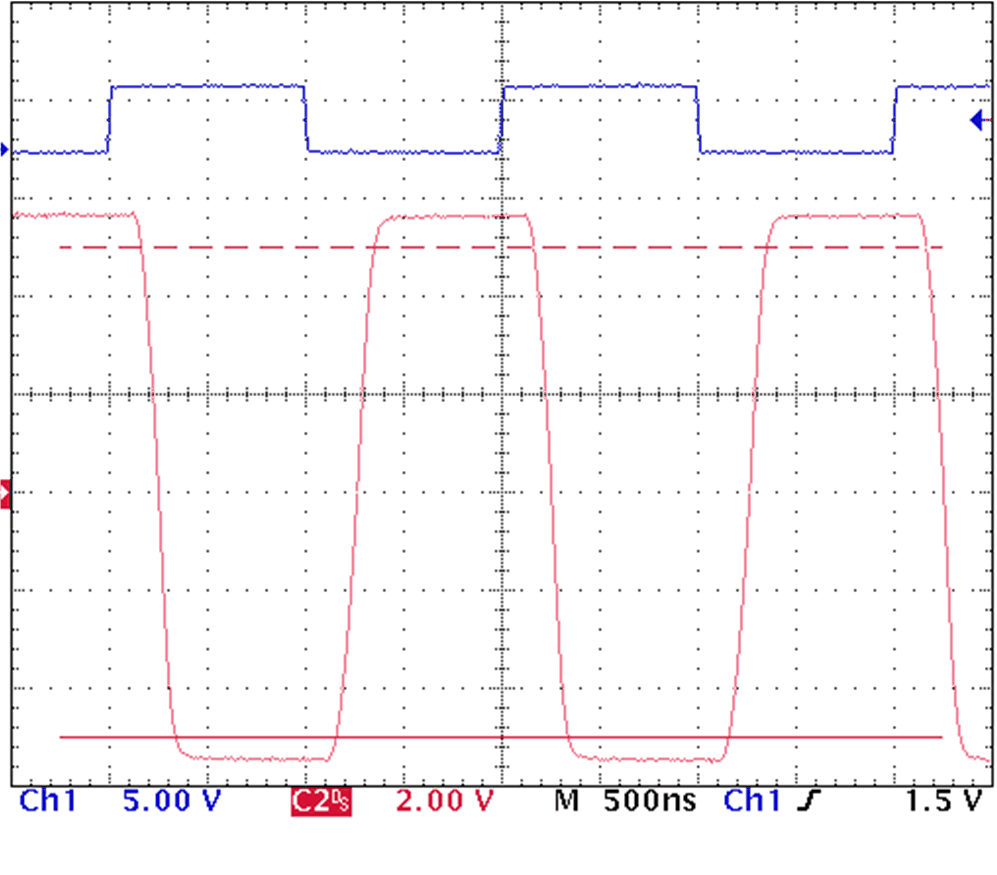
Driver input as top waveform and driver output as bottom waveform.
- 3.3-V VCC
- 1000-kbit/s data rate
- 200-pF and 3-kΩ Load
 Figure 9. 1000-kbps Driver Timing Waveform