SCDS216E OCTOBER 2005 – November 2017 TS5A3160
PRODUCTION DATA.
- 1 Features
- 2 Applications
- 3 Description
- 4 Revision History
- 5 Pin Configuration and Functions
-
6 Specifications
- 6.1 Absolute Maximum Ratings
- 6.2 ESD Ratings
- 6.3 Recommended Operating Conditions
- 6.4 Thermal Information
- 6.5 Electrical Characteristics for 5-V Supply
- 6.6 Electrical Characteristics for 3.3-V Supply
- 6.7 Electrical Characteristics for 2.5-V Supply
- 6.8 Electrical Characteristics for 1.8-V Supply
- 6.9 Typical Characteristics
- 7 Parameter Measurement Information
- 8 Detailed Description
- 9 Application and Implementation
- 10Power Supply Recommendations
- 11Layout
- 12Device and Documentation Support
- 13Mechanical, Packaging, and Orderable Information
Package Options
Mechanical Data (Package|Pins)
Thermal pad, mechanical data (Package|Pins)
- DCK|6
Orderable Information
1 Features
- Low ON-State Resistance (1 Ω)
- Isolation in the Powered-Off Mode, V+ = 0
- Specified Make-Before-Break Switching
- Control Inputs are 5-V Tolerant
- Low Charge Injection
- Excellent ON-Resistance Matching
- Low Total Harmonic Distortion
- 1.65-V to 5.5-V Single-Supply Operation
- Latch-Up Performance Exceeds 100 mA
Per JESD 78, Class II - ESD Performance Tested Per JESD 22
- 2000-V Human Body Model
(A114-B, Class II) - 1000-V Charged-Device Model (C101)
- 2000-V Human Body Model
2 Applications
- Mobile Phones
- Consumer and Computing
- Portable Instrumentation
3 Description
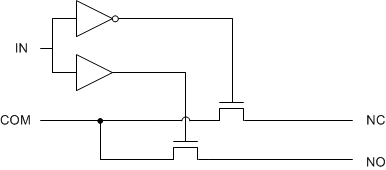
The TS5A3160 device is a single-pole double-throw (SPDT) analog switch that is designed to operate from 1.65 V to 5.5 V. The device offers a low ON-state resistance and an excellent channel-to-channel ON-state resistance matching. The device has excellent total harmonic distortion (THD) performance and consumes very low power. These features make this device suitable for portable audio applications.
Device Information(1)
| PART NUMBER | PACKAGE | BODY SIZE (NOM) |
|---|---|---|
| TS5A3160DBV | SOT-23 (6) | 2.90 mm × 1.60 mm |
| TS5A3160DCK | SC70 (6) | 2.00 mm × 1.25 mm |
- For all available packages, see the orderable addendum at the end of the data sheet.
Block Diagram
