SLLSF13B June 2017 – May 2019 TUSB1046A-DCI
PRODUCTION DATA.
- 1 Features
- 2 Applications
- 3 Description
- 4 Revision History
- 5 Pin Configuration and Functions
-
6 Specifications
- 6.1 Absolute Maximum Ratings
- 6.2 ESD Ratings
- 6.3 Recommended Operating Conditions
- 6.4 Thermal Information
- 6.5 Power Supply Characteristics
- 6.6 DC Electrical Characteristics
- 6.7 AC Electrical Characteristics
- 6.8 DCI Specific Electrical Characteristics
- 6.9 Timing Requirements
- 6.10 Switching Characteristics
- 6.11 Typical Characteristics
- 7 Parameter Measurement Information
-
8 Detailed Description
- 8.1 Overview
- 8.2 Functional Block Diagram
- 8.3 Feature Description
- 8.4 Device Functional Modes
- 8.5 Programming
- 8.6
Register Maps
- 8.6.1 General Register (address = 0x0A) [reset = 00000001]
- 8.6.2 DisplayPort Control/Status Registers (address = 0x10) [reset = 00000000]
- 8.6.3 DisplayPort Control/Status Registers (address = 0x11) [reset = 00000000]
- 8.6.4 DisplayPort Control/Status Registers (address = 0x12) [reset = 00000000]
- 8.6.5 DisplayPort Control/Status Registers (address = 0x13) [reset = 00000000]
- 8.6.6 USB3.1 Control/Status Registers (address = 0x20) [reset = 00000000]
- 8.6.7 USB3.1 Control/Status Registers (address = 0x21) [reset = 00000000]
- 8.6.8 USB3.1 Control/Status Registers (address = 0x22) [reset = 00000100]
- 9 Application and Implementation
- 10Power Supply Recommendations
- 11Layout
- 12Device and Documentation Support
- 13Mechanical, Packaging, and Orderable Information
Package Options
Mechanical Data (Package|Pins)
- RNQ|40
Thermal pad, mechanical data (Package|Pins)
Orderable Information
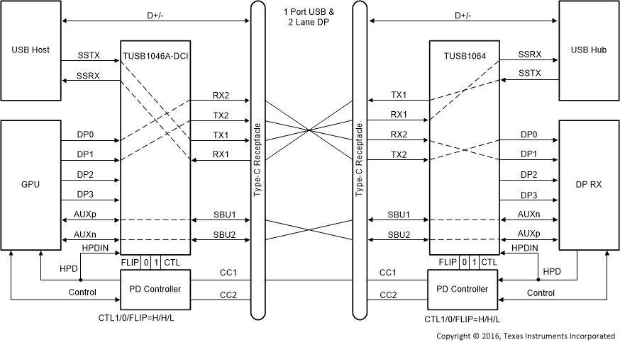
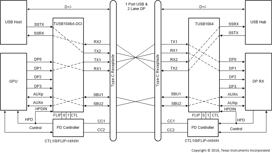
9.3.2 USB 3.1 and 2 Lanes of DisplayPort
The TUSB1046-DCI operates in USB3.1 and 2 Lanes of DisplayPort mode when the CTL1 pin is high and CTL0 pin is high.
 Figure 32. USB3.1 + 2 Lane DP – No Flip (CTL1 = H, CTL0 = H, FLIP = L)
  Figure 33. USB 3.1 + 2 Lane DP – Flip (CTL1 = H, CTL0 = H, FLIP = H)