SLLSEK3E July 2015 – September 2017 TUSB4041I
PRODUCTION DATA.
- 1 Features
- 2 Applications
- 3 Description
- 4 Revision History
- 5 Description (continued)
- 6 Pin Configuration and Functions
- 7 Specifications
-
8 Detailed Description
- 8.1 Overview
- 8.2 Functional Block Diagram
- 8.3 Feature Description
- 8.4 Device Functional Modes
- 8.5
Register Maps
- 8.5.1 Configuration Registers
- 8.5.2 ROM Signature Register
- 8.5.3 Vendor ID LSB Register
- 8.5.4 Vendor ID MSB Register
- 8.5.5 Product ID LSB Register
- 8.5.6 Product ID MSB Register
- 8.5.7 Device Configuration Register
- 8.5.8 Battery Charging Support Register
- 8.5.9 Device Removable Configuration Register
- 8.5.10 Port Used Configuration Register
- 8.5.11 Device Configuration Register 2
- 8.5.12 USB 2.0 Port Polarity Control Register
- 8.5.13 UUID Byte N Register
- 8.5.14 Language ID LSB Register
- 8.5.15 Language ID MSB Register
- 8.5.16 Serial Number String Length Register
- 8.5.17 Manufacturer String Length Register
- 8.5.18 Product String Length Register
- 8.5.19 Serial Number String Registers
- 8.5.20 Manufacturer String Registers
- 8.5.21 Product String Byte N Register
- 8.5.22 Additional Feature Configuration Register
- 8.5.23 Device Status and Command Register
-
9 Application and Implementation
- 9.1 Application Information
- 9.2
Typical Application
- 9.2.1 Design Requirements
- 9.2.2
Detailed Design Procedure
- 9.2.2.1 Upstream Port Implementation
- 9.2.2.2 Downstream Port 1 Implementation
- 9.2.2.3 Downstream Port 2 Implementation
- 9.2.2.4 Downstream Port 3 Implementation
- 9.2.2.5 Downstream Port 4 Implementation
- 9.2.2.6 VBUS Power Switch Implementation
- 9.2.2.7 Clock, Reset, and Miscellaneous
- 9.2.2.8 TUSB4041I Power Implementation
- 9.2.3 Application Curves
- 10Power Supply Recommendations
- 11Layout
- 12Device and Documentation Support
- 13Mechanical, Packaging, and Orderable Information
Package Options
Refer to the PDF data sheet for device specific package drawings
Mechanical Data (Package|Pins)
- PAP|64
Thermal pad, mechanical data (Package|Pins)
Orderable Information
1 Features
- Four Port USB 2.0 Hub
- USB 2.0 Hub Features
- Multi Transaction Translator (MTT) Hub: Four Transaction Translators
- Four Asynchronous Endpoint Buffers per Transaction Translator
- Supports USB Battery Charging
- CDP Mode (Upstream Port Connected)
- DCP Mode (Upstream Port Unconnected)
- DCP Mode Complies With Chinese Telecommunications Industry Standard YD/T 1591-2009
- Supports D+ and D– Divider Mode
- Per Port or Ganged Power Switching and Overcurrent Notification Inputs
- OTP ROM, Serial EEPROM or I2C and SMBus Slave Interface for Custom Configurations:
- VID and PID
- Customizable Ports
- Manufacturer and Product Strings (not by OTP ROM)
- Serial Number (not by OTP ROM)
- Application Feature Selection Using Pin Selection or EEPROM, I2C, or SMBus Slave Interface
- Provides 128-Bit Universally Unique Identifier (UUID)
- Supports On-Board and In-System OTP and EEPROM Programming Through the USB 2.0 Upstream Port
- Single Clock Input, 24-MHz Crystal or Oscillator
- DM/DP Polarity Swap
- Type C Compatible
- No Special Driver Requirements; Works Seamlessly on any Operating System With USB Stack Support
- 64-Pin HTQFP Package (PAP)
2 Applications
- Computer Systems
- Docking Stations
- Monitors
- Set-Top Boxes
3 Description
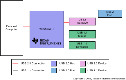
The TUSB4041I device is a four-port USB 2.0 hub. The device provides USB high-speed or full-speed connections on the upstream port. The device also provides USB high-speed, full-speed, or low-speed connections on the downstream ports. When the upstream port is connected to an electrical environment that only supports high-speed, full-speed, and low-speed connections, the USB high-speed, full-speed and low-speed connectivity is enabled on the downstream ports. When the upstream port is connected to an electrical environment that only supports full-speed or low-speed connections, the USB high-speed connectivity are disabled on the downstream ports.
Device Information(1)
| PART NUMBER | PACKAGE | BODY SIZE (NOM) |
|---|---|---|
| TUSB4041I | HTQFP (64) | 10.00 mm × 10.00 mm |
- For all available packages, see the orderable addendum at the end of the data sheet.
