SLLSE67I March 2011 – March 2016 TUSB9261
PRODUCTION DATA.
- 1 Features
- 2 Applications
- 3 Description
- 4 Revision History
- 5 Pin Configuration and Functions
- 6 Specifications
- 7 Detailed Description
- 8 Application and Implementation
- 9 Power Supply Recommendations
- 10Layout
- 11Device and Documentation Support
- 12Mechanical, Packaging, and Orderable Information
Package Options
Mechanical Data (Package|Pins)
- PVP|64
Thermal pad, mechanical data (Package|Pins)
- PVP|64
Orderable Information
7 Detailed Description
7.1 Overview
The major functional blocks are as follows:
- Cortex M3 microcontroller subsystem including the following peripherals:
- Time interrupt modules, including watchdog timer
- Universal asynchronous receive/transmit (SCI)
- SPI
- General purpose input/output (GPIO)
- PWM for support of PWM outputs (PWM)
- USB 3.0 core (endpoint controller) and integrated USB 3.0 PHY
- AHCI-compliant SATA controller and integrated SATA PHY
- Supporting Gen1i, Gen1m, Gen2i, and Gen2m
- Chip level clock generation and distribution
- Support for JTAG 1149.1 and 1149.6
7.2 Functional Block Diagram

7.3 Feature Description
7.3.1 Operation
7.3.1.1 General Functionality
The TUSB9261 ROM contains boot code that executes after a global reset, which performs the initial configuration required to load a firmware image from an attached SPI flash memory to local RAM.
After the firmware is loaded, it configures the SATA advanced host controller interface host bus adapter (AHCI) and the USB device controller. In addition, the configuration of the AHCI includes a port reset, which initiates an out of band (OOB) TX sequence from the AHCI link layer to determine if a device is connected, and if so, negotiate the connection speed with the device (3.0 Gbps or 1.5 Gbps).
The configuration of the USB device controller includes creation of the descriptors, configuration of the device endpoints for support of UASP and USB mass storage class BOT, allocation of memory for the transmit request blocks (TRBs), and creation of the TRBs necessary to transmit and receive packet data over the USB. In addition, the firmware provides any other custom configuration required for application-specific implementation, for example, a HID interface for user initiated backup.
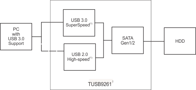
After the USB device controller configuration is complete, if a SATA device was detected during the AHCI configuration, the firmware connects the device to the USB bus when VBUS is detected. According to the USB 3.0 specification, the TUSB9261 initially tries to connect at SuperSpeed USB. If successful, it enters U0; otherwise, after the training time out, it enables the DP pullup and connects as a USB 2.0 high-speed or full-speed device depending on the speed supported by host or hub port.
When connected, the firmware presents the BOT interface as the primary interface and the UASP interface as the secondary interface. If the host stack is UASP aware, it can enable the UASP interface using a SET_INTERFACE request for alternate interface 1.
Following speed negotiation, the device should transmit a device to host (D2H) FIS with the device signature. This first D2H FIS is received by the link layer and copied to the port signature register. When firmware is notified of the device connection, it queries the device for capabilities using the IDENTIFY DEVICE command. Firmware then configures the device as appropriate for its interface and features supported, for example, an HDD that supports native command queuing (NCQ).
7.3.1.2 Firmware Support
Default firmware support is provided for the following:
- SuperSpeed USB and USB 2.0 high speed and full speed
- USB attached SCSI protocol (UASP)
- USB mass storage class (MSC) bulk-only transport (BOT)
- Including the 13 error cases
- USB mass storage specification for bootability
- USB device class definition for HID
- Firmware update and custom functionality (for example, one-touch backup)
- Serial ATA advanced host controller interface (AHCI)
- GPIO
- LED control and custom functions (for example, one-touch backup control)
- PWM
- LED dimming control
- SPI
- Firmware storage and storing custom device descriptors
- Serial communications interface (SCI)
- Debug output only
7.3.1.3 GPIO/PWM LED Designations
The default firmware provided by TI drives the GPIO and PWM outputs as listed in Table 1.
Table 1. GPIO/PWM LED Designations
The LEDs on the TUSB9261 product development kit (PDK) board are connected as in Table 1. See the TUSB9261 PDK Guide for more information on GPIO LED connection and usage. This EVM is available for purchase. Contact TI for ordering information.
7.3.1.4 Power-Up and Reset Sequence
The core power (VDD) must be present and at its minimum high level prior to, or at the same time that, the I/O power (VDD33).
In addition, meet the following constraints:
- All maximum ratings and recommended operating conditions are observed.
- All warnings about exposure to maximum rated and recommended conditions are observed, particularly junction temperature. These apply to power transitions as well as normal operation.
- Bus contention while VDD33 is powered up must be limited to 100 hours over the projected lifetime of the device.
- Bus contention while VDD33 is powered down may violate the absolute maximum ratings.
A supply bus is powered up when the voltage is within the recommended operating range. It is powered down when it is below that range, either stable or in transition.
A minimum reset duration of 2 ms is required. This is defined as the time when the power supplies are in the recommended operating range to the deassertion of GRSTz.
7.3.2 Clock Connections
7.3.2.1 Clock Source Requirements
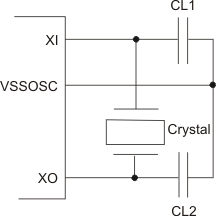
The TUSB9261 supports an external oscillator source or a crystal unit. If a clock is provided to XI instead of a crystal, XO is left open and VSSOSC should be connected to the PCB ground plane. Otherwise, if a crystal is used, the connection needs to follow these guidelines.
Because XI and XO are coupled to other leads and supplies on the PCB, it is important to keep them as short as possible and away from any switching leads. TI also recommends to minimize the capacitance between XI and XO. This can be accomplished by connecting the VSSOSC lead to the two external capacitors CL1 and CL2 and shielding them with the clean ground lines. The VSSOSC should not be connected to PCB ground when using a crystal.
Load capacitance (Cload) of the crystal (varies with the crystal vendor) is the total capacitance value of the entire oscillation circuit system as seen from the crystal. It includes two external capacitors, CL1 and CL2, in Figure 1. The trace length between the decoupling capacitors and the corresponding power pins on the TUSB9261 must be minimized. TI also recommends that the trace length from the capacitor pad to the power or ground plane be minimized.
 Figure 1. Typical Crystal Connections
7.3.2.2 Clock Source Selection Guide
Reference clock jitter is an important parameter. Jitter on the reference clock degrades both the transmit eye and receiver jitter tolerance no matter how clean the rest of the PLL is, thereby impairing system performance. Additionally, a particularly jittery reference clock may interfere with the PLL lock detection mechanism, forcing the lock detector to issue an Unlock signal. A good-quality, low-jitter reference clock is required to achieve compliance with supported USB3.0 standards. For example, USB3.0 specification requires the random jitter (RJ) component of either RX or TX to be 2.42 ps (random phase jitter calculated after applying jitter transfer function (JTF)). As the PLL typically has a number of additional jitter components, the reference clock jitter must be considerably below the overall jitter budget.
7.4 Device Functional Modes
7.4.1 VBUS Power
Power can be supplied by a USB cable on the terminal VBUS. When using power from VBUS, both the TUSB9261 and the SATA device are allowed to draw only up to 500 mA from VBUS when operating.
7.4.2 External Power
Power can be supplied from an external power source. When using an external power source, both the TUSB9261 and the SATA interface can draw all their current from the external supply.
7.4.3 External Voltage Regulator
Because the TUSB9261 requires two voltage supplies (1.1 V and 3.3 V), TI recommends a multi-channel voltage regulator. The TPS650061 or TPS65024x are good choices. The TPS650061 uses a DC-DC converter and two LDO regulators in a single package. The DC-DC converter can supply 1-A nominal current while the two LDOs can supply 300-mA nominal current. Because the 1.1-V supply can consume upwards of 340 mA of current, the DC-DC converter is ideal for supplying the 1.1-V current while the two LDOs can be used to supply 3.3-V current. Likewise the TPS65024x uses three DC-DC converters and three LDOs. Both devices also have a built-in supervisor circuit that can be connected to GRST on the TUSB9261.