SLLSE67I March 2011 – March 2016 TUSB9261
PRODUCTION DATA.
- 1 Features
- 2 Applications
- 3 Description
- 4 Revision History
- 5 Pin Configuration and Functions
- 6 Specifications
- 7 Detailed Description
- 8 Application and Implementation
- 9 Power Supply Recommendations
- 10Layout
- 11Device and Documentation Support
- 12Mechanical, Packaging, and Orderable Information
Package Options
Mechanical Data (Package|Pins)
- PVP|64
Thermal pad, mechanical data (Package|Pins)
- PVP|64
Orderable Information
10 Layout
10.1 Layout Guidelines
10.1.1 High-Speed Differential Routing
The high-speed differential pair (USB_DM and USB_DP) is connected to a USB type B connector. The differential pair traces should be routed with 90-Ω, ±15% differential impedance. The high-speed signal pair should be trace length matched. Maximum trace length mismatch between high-speed USB signal pairs should be no greater than 150 mils. Keep total trace length to a minimum. Route differential traces first. Route the differential pairs on the top or bottom layers with the minimum amount of vias possible. No termination or coupling capacitors are required. If a common-mode choke is required, then place the choke as close as possible to the USB connector signal pins. Likewise, ESD clamps should also be placed as close as possible to the USB connector signal pins (closer than the choke).
To minimize crosstalk on the USB2/3 differential signal pairs, TI recommends that the spacing between the two interfaces be five times the width of the trace (5W rule). For instance, if the SS USB TX/RX differential pair trace widths are 5 mils, then there should be 25 mils of space (air gap) between the TX and RX differential pairs and the DP/DM differential pair. If this 5W rule cannot be implemented, then the space between the TX/RX differential pairs and DP/DM differential pairs should be maximized as much as possible and ground-fill should be placed between the two. In this case, it is better to route each differential pair on opposite sides of the board with a ground plane between them.
10.1.2 SuperSpeed Differential Routing
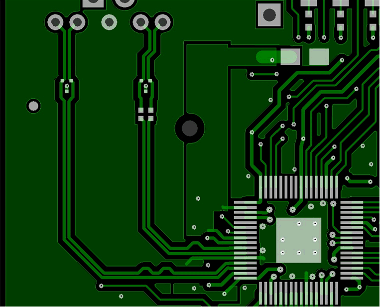
SuperSpeed consists of two differential routing pairs, a transmit pair (USB_SSTXM and USB_SSTXP) and a receive pair (USB_SSRXM and USB_SSRXP). Each differential pair’s traces should be routed with 90-Ω, ±15% differential impedance. The high-speed signal pair should be trace length matched. Maximum trace length mismatch between SuperSpeed USB signal pairs should be no greater than 2.5 mils. The transmit differential pair does not have to be the same length as the receive differential pair. Keep total trace length to a minimum. Route differential traces first. Route the differential pairs on the top or bottom layers with the minimum amount of vias possible. The transmitter differential pair requires 0.1-uF coupling capacitors for proper operation. The package/case size of these capacitors should be no bigger than 0402. C-packs are not allowed. The capacitors should be placed symmetrically as close as possible to the USB connector signal pins. If a common mode choke is required, then place the choke as close as possible to the USB connector signal pins (closer than the transmitter capacitors). Likewise ESD clamps should also be placed as close as possible to the USB connector signal pins (closer than the choke and transmitter capacitors).
It is permissible to swap the plus and minus on either or both of the SuperSpeed differential pairs. This may be necessary to prevent the differential traces from crossing over one another. However, it is not permissible to swap the transmitter differential pair with receive differential pair. To minimize crosstalk on the SS USB differential signal pairs, TI recommends that the spacing between the TX and RX signal pairs be five times the width of the trace (5W rule). For instance, if the SS USB TX/RX differential pair trace widths are 5 mils, then there should be 25 mils of space (air gap) between the TX and RX differential pairs.
If this 5W rule cannot be implemented, then the space between the TX and RX differential pairs should be maximized as much as possible and ground-fill should be placed between the two. In this case, it is better to route each differential pair on opposite sides of the board with a ground plane between them.
10.1.3 SATA Differential Routing
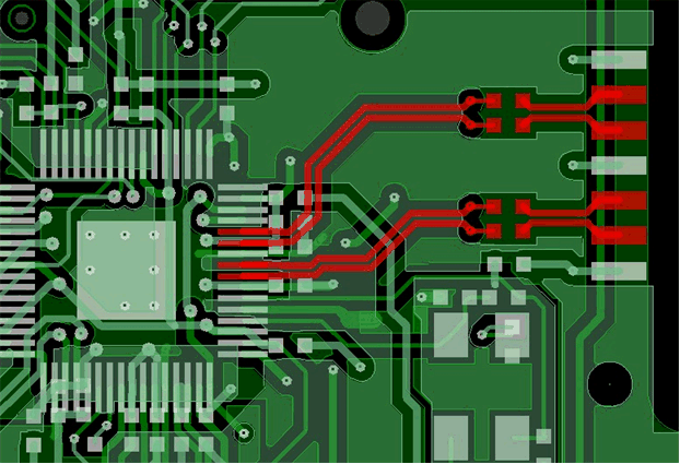
The SATA traces (SATA_TXP and SATA_TXM) should be routed with 100-Ω, ±15% differential impedance. Maximum trace length mismatch between SATA signal pairs should be no greater than 2.5 mils. The transmit differential pair does not have to be the same length as receive differential pair. Keep total trace length to a minimum. Route differential traces first. Route the differential pairs on the top or bottom layers with the minimum amount of vias possible. Each SATA trace requires a coupling capacitor be placed inline. The package/case size of these capacitors should be no bigger than 0402. C-packs are not allowed. The capacitors should be placed symmetrically as close as possible to the SATA connector signal pins.
It is permissible to swap the plus and minus on the SATA differential pair. This may be necessary to prevent the differential traces from crossing over one another. However, it is not permissible to swap the transmitter differential pair with the receive differential pair.
To minimize crosstalk on the SATA differential signal pairs, TI recommends that the spacing between the TX and RX signal pairs for each interface be five times the width of the trace (5W rule). For instance, if the SATA TX/RX differential pair trace widths are 5 mils, then there should be 25 mils of space (air gap) between the TX and RX differential pairs. If this 5W rule cannot be implemented, then the space between the TX and RX differential pairs should be maximized as much as possible and ground-fill should be placed between the two. In this case, it is better to route each differential pair on opposite sides of the board with a ground plane between them.
10.2 Layout Examples
 Figure 5. SuperSpeed Differential Routing
 Figure 6. SATA Differential Routing