SCES643H November 2006 – August 2020 TXB0108
PRODUCTION DATA
- 1 Features
- 2 Applications
- 3 Description
- 4 Revision History
- 5 Pin Configuration and Functions
-
6 Specifications
- 6.1 Absolute Maximum Ratings
- 6.2 Handling Ratings
- 6.3 Recommended Operating Conditions
- 6.4 Thermal Information
- 6.5 Electrical Characteristics
- 6.6 Timing Requirements: VCCA = 1.2 V
- 6.7 Timing Requirements: VCCA = 1.5 V ± 0.1 V
- 6.8 Timing Requirements: VCCA = 1.8 V ± 0.15 V
- 6.9 Timing Requirements: VCCA = 2.5 V ± 0.2 V
- 6.10 Timing Requirements: VCCA = 3.3 V ± 0.3 V
- 6.11 Switching Characteristics: VCCA = 1.2 V
- 6.12 Switching Characteristics: VCCA = 1.5 V ± 0.1 V
- 6.13 Switching Characteristics: VCCA = 1.8 V ± 0.15 V
- 6.14 Switching Characteristics: VCCA = 2.5 V ± 0.2 V
- 6.15 Switching Characteristics: VCCA = 3.3 V ± 0.3 V
- 6.16 Operating Characteristics
- 6.17 Typical Characteristics
- 7 Parameter Measurement Information
- 8 Detailed Description
- 9 Application and Implementation
- 10Power Supply Recommendations
- 11Layout
- 12Device and Documentation Support
- 13Mechanical, Packaging, and Orderable Information
Package Options
Refer to the PDF data sheet for device specific package drawings
Mechanical Data (Package|Pins)
- NME|20
- YZP|20
- DQS|20
- PW|20
- RGY|20
Thermal pad, mechanical data (Package|Pins)
Orderable Information
5 Pin Configuration and Functions
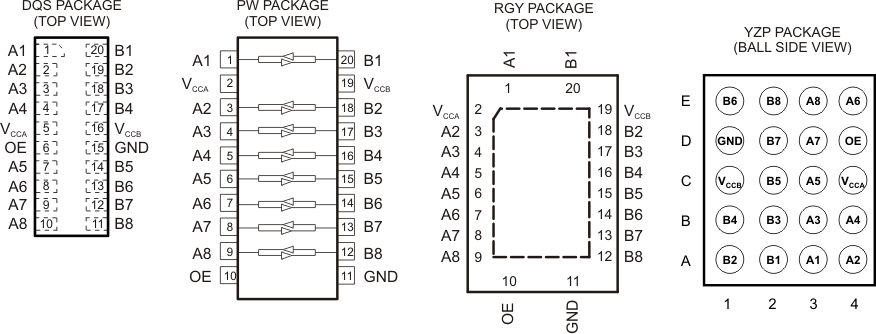
For the RGY package, the exposed center thermal pad must be connected to ground.
Pullup resistors are not required on both sides for Logic I/O.
If pullup or pulldown resistors are needed, the resistor value must be over 50 kΩ.
50 kΩ is a safe recommended value, if the customer can accept higher VOL or lower VOH, smaller pullup or pulldown resistor is allowed, the draft estimation is VOL = VCCOUT × 4.5 k/(4.5 k + RPU) and VOH = VCCOUT × RDW/(4.5 k + RDW).
If pullup resistors are needed, please refer to the TXS0108 or contact TI.
For detailed information, please refer to application note SCEA043.
") Figure 5-1 NME/GXY/ZXY
PACKAGE(BOTTOM VIEW)
Figure 5-1 NME/GXY/ZXY
PACKAGE(BOTTOM VIEW)Table 5-1 Pin Functions
| PIN | I/O(1) | FUNCTION | |||
|---|---|---|---|---|---|
| SIGNAL NAME |
PW, RGY NO. | DQS NO. | YZP GRID LOCATOR |
||
| A1 | 1 | 1 | A3 | I/O | Input/output 1. Referenced to VCCA. |
| VCCA | 2 | 5 | C4 | S | A-port supply voltage. 1.1 V ≤ VCCA ≤ 3.6 V, VCCA ≤ VCCB. |
| A2 | 3 | 2 | A4 | I/O | Input/output 2. Referenced to VCCA. |
| A3 | 4 | 3 | B3 | I/O | Input/output 3. Referenced to VCCA. |
| A4 | 5 | 4 | B4 | I/O | Input/output 4. Referenced to VCCA. |
| A5 | 6 | 7 | C3 | I/O | Input/output 5. Referenced to VCCA. |
| A6 | 7 | 8 | E4 | I/O | Input/output 6. Referenced to VCCA. |
| A7 | 8 | 9 | D3 | I/O | Input/output 7. Referenced to VCCA. |
| A8 | 9 | 10 | E3 | I/O | Input/output 8. Referenced to VCCA. |
| OE | 10 | 6 | D4 | I | Output enable. Pull OE low to place all outputs in 3-state mode. Referenced to VCCA. |
| GND | 11 | 15 | D1 | S | Ground |
| B8 | 12 | 11 | E2 | I/O | Input/output 8. Referenced to VCCB. |
| B7 | 13 | 12 | D2 | I/O | Input/output 7. Referenced to VCCB. |
| B6 | 14 | 13 | E1 | I/O | Input/output 6. Referenced to VCCB. |
| B5 | 15 | 14 | C2 | I/O | Input/output 5. Referenced to VCCB. |
| B4 | 16 | 17 | B1 | I/O | Input/output 4. Referenced to VCCB. |
| B3 | 17 | 18 | B2 | I/O | Input/output 3. Referenced to VCCB. |
| B2 | 18 | 19 | A1 | I/O | Input/output 2. Referenced to VCCB. |
| VCCB | 19 | 16 | C1 | S | B-port supply voltage. 1.65 V ≤ VCCB ≤ 5.5 V. |
| B1 | 20 | 20 | A2 | I/O | Input/output 1. Referenced to VCCB. |
| Thermal Pad | — | — | For the RGY package, the exposed center thermal pad must be connected to ground. | ||
(1) I = input, O = output, I/O = input and output, S = power supply
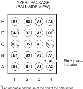
Table 5-2 Pin Assignments (20-Ball
NME/GXY/ZXY Package)
| 1 | 2 | 3 | 4 | 5 | |
|---|---|---|---|---|---|
| D | VCCB | B2 | B4 | B6 | B8 |
| C | B1 | B3 | B5 | B7 | GND |
| B | A1 | A3 | A5 | A7 | OE |
| A | VCCA | A2 | A4 | A6 | A8 |