SLVS056P May 1976 – January 2015
PRODUCTION DATA.
- 1 Features
- 2 Applications
- 3 Description
- 4 Simplified Schematic
- 5 Revision History
- 6 Pin Configuration and Functions
-
7 Specifications
- 7.1 Absolute Maximum Ratings
- 7.2 ESD Ratings
- 7.3 Recommended Operating Conditions
- 7.4 Thermal Information
- 7.5 Electrical Characteristics — uA7805
- 7.6 Electrical Characteristics — uA7808
- 7.7 Electrical Characteristics — uA7810
- 7.8 Electrical Characteristics — uA7812
- 7.9 Electrical Characteristics — uA7815
- 7.10 Electrical Characteristics — uA7824
- 7.11 Typical Characteristics
- 8 Detailed Description
- 9 Application and Implementation
- 10Power Supply Recommendations
- 11Layout
- 12Device and Documentation Support
- 13Mechanical, Packaging, and Orderable Information
Package Options
Mechanical Data (Package|Pins)
Thermal pad, mechanical data (Package|Pins)
- KTT|3
Orderable Information
9 Application and Implementation
NOTE
Information in the following applications sections is not part of the TI component specification, and TI does not warrant its accuracy or completeness. TI’s customers are responsible for determining suitability of components for their purposes. Customers should validate and test their design implementation to confirm system functionality.
9.1 Application Information
The following section shows application details of the µA78xx as a linear regulator.
9.2 Typical Application
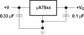 Figure 2. Fixed-Output Regulator
9.2.1 Design Requirements
- Input supply capacitor recommended for filtering noise on the input
- Output supply decoupling capacitor for stabilizing the output
9.2.2 Detailed Design Procedure
9.2.2.1 Operation With a Load Common to a Voltage of Opposite Polarity
In many cases, a regulator powers a load that is not connected to ground but, instead, is connected to a voltage source of opposite polarity (e.g., operational amplifiers, level-shifting circuits, etc.). In these cases, a clamp diode should be connected to the regulator output as shown in Figure 3. This protects the regulator from output polarity reversals during startup and short-circuit operation.
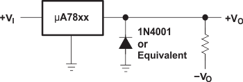 Figure 3. Output Polarity-Reversal-Protection Circuit
9.2.2.2 Reverse-Bias Protection
Occasionally, the input voltage to the regulator can collapse faster than the output voltage. This can occur, for example, when the input supply is crowbarred during an output overvoltage condition. If the output voltage is greater than approximately 7 V, the emitter-base junction of the series-pass element (internal or external) could break down and be damaged. To prevent this, a diode shunt can be used as shown in Figure 4.
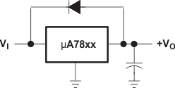 Figure 4. Reverse-Bias-Protection Circuit
9.2.3 Application Curves
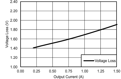 Figure 5. µA7805 Voltage Loss vs Output Current at 25°C
9.2.4 General Configurations
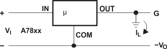 Figure 6. Positive Regulator in Negative Configuration (VI Must Float)
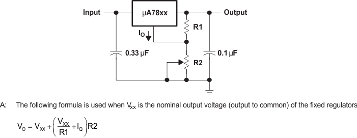 Figure 7. Adjustable-Output Regulator
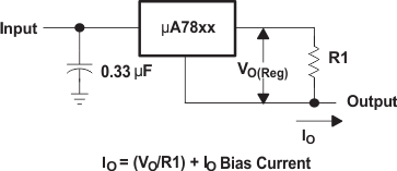 Figure 8. Current Regulator
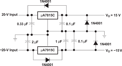 Figure 9. Regulated Dual Supply