SLUS157Q December 1999 – October 2019 UCC1895 , UCC2895 , UCC3895
PRODUCTION DATA.
- 1 Features
- 2 Applications
- 3 Description
- 4 Revision History
- 5 Pin Configuration and Functions
- 6 Specifications
-
7 Detailed Description
- 7.1 Overview
- 7.2 Functional Block Diagrams
- 7.3
Feature Description
- 7.3.1 ADS (Adaptive Delay Set)
- 7.3.2 CS (Current Sense)
- 7.3.3 CT (Oscillator Timing Capacitor)
- 7.3.4 DELAB and DELCD (Delay Programming Between Complementary Outputs)
- 7.3.5 EAOUT, EAP, and EAN (Error Amplifier)
- 7.3.6 OUTA, OUTB, OUTC, and OUTD (Output MOSFET Drivers)
- 7.3.7 PGND (Power Ground)
- 7.3.8 RAMP (Inverting Input of the PWM Comparator)
- 7.3.9 REF (Voltage Reference)
- 7.3.10 RT (Oscillator Timing Resistor)
- 7.3.11 GND (Analog Ground)
- 7.3.12 SS/DISB (Soft Start/Disable)
- 7.3.13 SYNC (Oscillator Synchronization)
- 7.3.14 VDD (Chip Supply)
- 7.4 Device Functional Modes
- 7.5 Programming
-
8 Application and Implementation
- 8.1 Application Information
- 8.2
Typical Application
- 8.2.1 Design Requirements
- 8.2.2
Detailed Design Procedure
- 8.2.2.1 Power Loss Budget
- 8.2.2.2 Preliminary Transformer Calculations (T1)
- 8.2.2.3 QA, QB, QC, QD FET Selection
- 8.2.2.4 Selecting LS
- 8.2.2.5 Selecting Diodes DB and DC
- 8.2.2.6 Output Inductor Selection (LOUT)
- 8.2.2.7 Output Capacitance (COUT)
- 8.2.2.8 Select Rectifier Diodes
- 8.2.2.9 Input Capacitance (CIN)
- 8.2.2.10 Current Sense Network (CT, RCS, RR, DA)
- 8.2.3 Application Curves
- 9 Power Supply Recommendations
- 10Layout
- 11Device and Documentation Support
- 12Mechanical, Packaging, and Orderable Information
Package Options
Mechanical Data (Package|Pins)
Thermal pad, mechanical data (Package|Pins)
Orderable Information
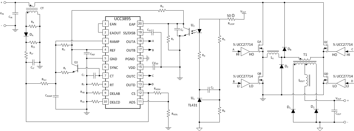
8.2 Typical Application
A typical application for the UCC3895 device is a controller for a phase-shifted full-bridge converter that converts a 390-VDC input to a regulated 12-V output.
 Figure 18. UCC3895 Typical Application