SLUSA87C August 2010 – October 2015 UCC24610
PRODUCTION DATA.
- 1 Features
- 2 Applications
- 3 Description
- 4 Revision History
- 5 Pin Configuration and Functions
- 6 Specifications
- 7 Detailed Description
-
8 Application and Implementation
- 8.1 Application Information
- 8.2
Typical Application
- 8.2.1 Design Requirements
- 8.2.2 Detailed Design Procedure
- 8.2.3 Application Curves
- 9 Power Supply Recommendations
- 10Layout
- 11Device and Documentation Support
- 12Mechanical, Packaging, and Orderable Information
Package Options
Mechanical Data (Package|Pins)
Thermal pad, mechanical data (Package|Pins)
- DRB|8
Orderable Information
7 Detailed Description
7.1 Overview
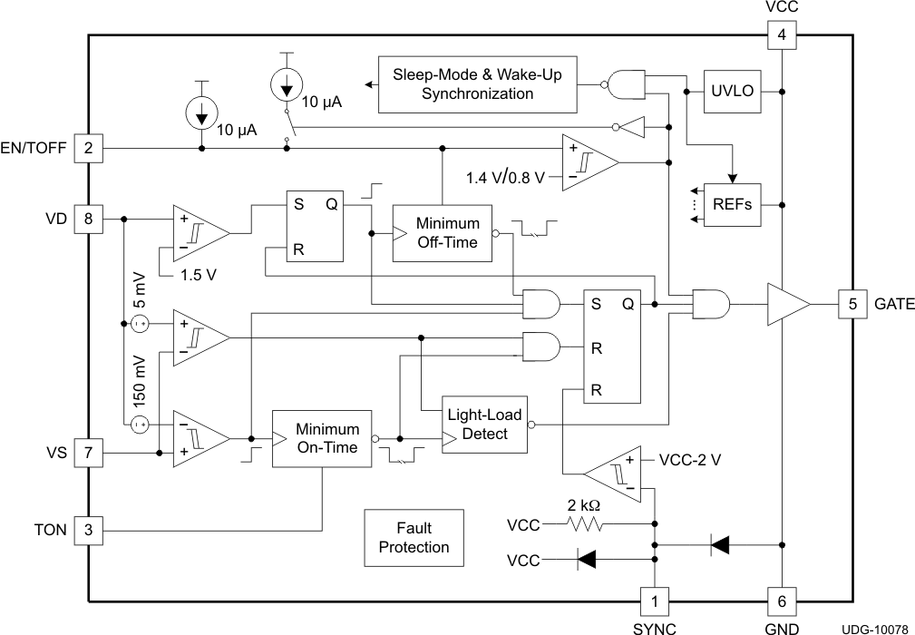
The UCC24610 synchronous rectifier (SR) controller uses drain-to-source voltage sensing to determine the SR MOSFET conduction interval. The SR MOSFET is turned on when VDS exceeds –150 mV, and is turned off when VDS diminishes to –5 mV or the SYNC input is triggered for CCM operation. Programmable minimum on-time and off-time helps avoid false turnon and turnoff responses to switch voltage ringing and noise. To reduce light-load switching losses, automatic light-load mode disables the GATE pulses when the actual on-time based on VDS becomes less than the programmed minimum on-time. When the load increases such that the conduction time exceeds the programmed minimum on-time, the controller resumes normal SR operation.
7.2 Functional Block Diagram

7.3 Feature Description
7.3.1 Normal Operation
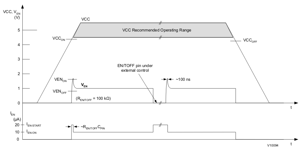
The UCC24610 GREEN rectifier synchronous-rectifier (SR) controller powers up into UVLO mode as VCC increases from 0 V. Enable current (IEN) from the EN/TOFF pin is inhibited until VCC exceeds the VCC(on) threshold, and remains active as long as VCC exceeds the VCC(off) threshold. The voltage on the EN/TOFF pin determines whether the controller is enabled or not. The controller operates in the normal run mode when the enable voltage (VEN) exceeds the enable threshold VEN(on) and remains enabled as long as VEN exceeds the VEN(off) threshold.
After the controller is enabled, VEN programs the minimum off time inversely proportional to the voltage (see Enabling and TOFF Programming). The two-state enable current allows a lower-value resistance for REN(off) (necessary to program longer off time) to still generate sufficient voltage to exceed VEN(on) at start-up. A simple resistor from EN/TOFF to GND generates VEN based on the level of IEN current flowing through it (see Figure 17). Alternatively, VEN may be driven by an external voltage source provided this voltage exceeds VEN(on) for at least 100 ns before settling to its final programming level.
 Figure 17. Behavior of IEN and VEN as VCC Varies (REN/TOFF = 100 kΩ)
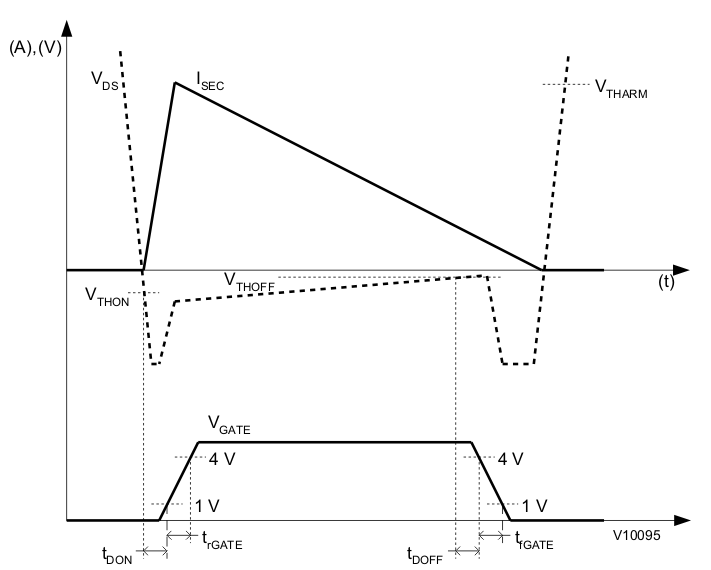
The UCC24610 SR controller determines the conduction time of the SR-MOSFET by comparing the drain-to-source voltage of the MOSFET against a turnon threshold and a turnoff threshold. The GATE output is driven high when VDS of the MOSFET exceeds VTH(on) and is driven low when VDS decreases below VTH(off) as illustrated in Figure 18.
 Figure 18. GATE Output With Respect to VDS
NOTE
Because of finite propagation and rise times, the body diode of the SR-MOSFET may conduct briefly after VTH(on) has been exceeded. Also, the body-diode conducts the residual secondary current after VTH(off) has been crossed. A waveform similar to that of VDS depicted in Figure 18 can be observed during SR operation in a simple flyback circuit.
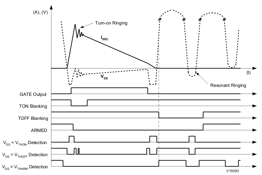
However, actual in-circuit waveforms are rarely as clean as shown in Figure 18. Instead, parasitic inductances and capacitances set up resonant ringing at various inflection points in the waveforms. The UCC24610 has control timing and programming options that help avoid interference from such ringing with proper operation. Figure 19 shows more realistic waveforms and the internal control timing which accommodates them. The waveforms affecting the SR-MOSFET in a typical flyback circuit are shown.
 Figure 19. Internal Signal Timing With Respect to Realistic DCM Waveforms
Minimum on-time TON is programmed with a resistor from TON, (pin 3) to GND to blank the response of the turnoff detection circuit to prevent GATE from being turned off from spurious crossings of VTH(off) due to noise and ringing. TON is triggered by the GATE turning on. Refer to TON Programming for details.
Minimum off-time TOFF is programmed with a resistor from pin 2 to GND to blank the response of the turnon detection circuit to prevent GATE from being turned-on again from spurious crossings of VTH(on) due to excessive COSS resonant ringing. TOFF is triggered by VDS crossing VTHARM after the GATE turns off. Refer to the Enabling and TOFF Programming for details
The GATE output may only turn on when the controller has been armed for the switching cycle. The controller is armed for each successive SR cycle only after TOFF expires. In high-frequency applications, an excessively long TOFF may interfere with timely turn-on of GATE in the next switching cycle. GATE turn on will be delayed if TOFF from the previous cycle has not yet expired.
7.3.2 Light-Load Operation
During normal operation, the synchronous rectifier conduction time is longer than the programmed minimum on-time. If load current decreases enough that the SR conduction time becomes shorter than the programmed minimum on-time, a light-load condition is detected. The light-load latch is set and the next GATE output pulse is blanked, so only the body diode of the controlled MOSFET conducts. This comparison between SR conduction time and minimum on time occurs every switching cycle, regardless of whether the GATE output pulse is enabled or blanked. When load current increases enough that the body-diode conduction time becomes longer than the programmed minimum on time, the light-load latch is cleared and the next GATE output pulse is enabled and the controlled MOSFET resumes SR operation.
Figure 20 depicts the progression into light-load mode for a DCM flyback application as the load decreases, while Figure 21 depicts the reverse progression back to run mode.
 Figure 20. Decreasing Load Current Progression Leads to Light-Load-Mode Operation
 Figure 21. Increasing Load Current Progression Returns to Run-Mode Operation
7.4 Device Functional Modes
7.4.1 UVLO Mode
When the VCC voltage to the device has not yet reached the VCC(on) threshold, or has fallen below the UVLO threshold VCC(off), the device operates in the low-power UVLO mode. In this mode, most internal functions are disabled and ICC current is typically much less than 100 µA. While in this mode, the EN current source is shut off, an internal 10-kΩ resistance is applied from the EN/TOFF pin to GND, the voltage on EN/TOFF is irrelevant, and the GATE output is driven low continuously for all VCC > 1.2 V. The device passes out of UVLO mode when VCC increases above the VCC(on) threshold. UVLO mode is very similar to Sleep mode, except VCC current is at ICC(start) level.
7.4.2 Sleep Mode
Sleep mode is a low-power operating mode similar to UVLO mode, except that this mode is entered under external control by forcing VEN below the VEN(off) threshold. Sleep mode may be used to reduce device operating losses to less than 1 mW. VCC current reduces to ICC(stby) level. External control overrides any internal timing conditions, and immediately forces the GATE output low and enters Sleep mode. Many internal circuits are turned off to reduce power consumption. When VEN is restored to above the VEN(on) threshold, the device exits Sleep mode synchronously into Light-load mode after a delay of approximately 25 µs to allow re-powered internal circuits to settle.
7.4.3 Run Mode
Run mode is the normal operating mode of the controller when not in UVLO mode, sleep mode, or light-load mode. In this mode, VCC current is higher because all internal control and timing functions are operating and the GATE output is driving the controlled MOSFET for synchronous rectification. VCC current is the sum of ICC(on) plus the average current necessary to drive the load on the GATE output. GATE output duty-cycle is dependent upon system line and load conditions, programmed TON and TOFF times, and SYNC-pulse timing (if applicable).
7.4.4 Light-Load Mode
Light-load mode is a low-power operating mode similar to sleep mode, except that this mode is entered automatically based on internal timing conditions. Light-load mode automatically reduces switching losses under light-load conditions by suppressing GATE output pulses whenever the detected synchronous conduction time is less than the programmed minimum on-time (TON). VCC current reduces to ICC(on) level. While in light-load mode, the MOSFET body-diode conduction time is still continuously monitored. When this time is detected to once again exceed TON, the device resumes run mode on the next switching cycle.
7.4.5 Fault Mode and Other Protections
Fault mode is a self-protection operating mode of the controller when certain types of single-fault conditions are detected on certain pins. In this mode, the device enters a shut-down state (not sleep mode) and drives the GATE output low. Specifically, Fault mode is entered if RTON > 301 kΩ or if RTON < 8.7 kΩ. Fault mode prevents the conditions of excessive or indefinite on-time (such as from an open-pin) and of excessive TON current (such as from a shorted-pin).
Similar protection is provided for the EN/TOFF pin. While not specifically detected as faults, if this pin becomes open-circuited TOFF defaults to a minimum value of ≈0.65 µs, and if shorted-to-GND the device enters sleep mode. Additionally, if the SYNC input is continuously held below its trigger threshold voltage, the GATE output is held low for the entire duration that SYNC remains in that condition.