SLUSA87C August 2010 – October 2015 UCC24610
PRODUCTION DATA.
- 1 Features
- 2 Applications
- 3 Description
- 4 Revision History
- 5 Pin Configuration and Functions
- 6 Specifications
- 7 Detailed Description
-
8 Application and Implementation
- 8.1 Application Information
- 8.2
Typical Application
- 8.2.1 Design Requirements
- 8.2.2 Detailed Design Procedure
- 8.2.3 Application Curves
- 9 Power Supply Recommendations
- 10Layout
- 11Device and Documentation Support
- 12Mechanical, Packaging, and Orderable Information
Package Options
Mechanical Data (Package|Pins)
Thermal pad, mechanical data (Package|Pins)
- DRB|8
Orderable Information
6 Specifications
6.1 Absolute Maximum Ratings
over operating free-air temperature range (unless otherwise noted) (1)| MIN | MAX | UNIT | ||
|---|---|---|---|---|
| Input voltage (6) | VCC | –0.3 | 6.5 | V |
| EN/TOFF(2) | –0.3 | VCC | V | |
| TON(3) | –0.3 | VCC | V | |
| VD for IVD ≤ –10 mA | –1.0 | 50 | V | |
| VS for IVS ≤ –10 mA | –1.0 | 0.5 | V | |
| Input current, peak | SYNC(4) pulsed, tPULSE ≤ 4 ms, duty cycle ≤ 1% | ±100 | mA | |
| Output current, peak | GATE(5) pulsed, tPULSE ≤ 4 ms, duty cycle ≤ 1% | ±3 | A | |
| TJ | Operating junction temperature | –40 | 125 | °C |
| Tstg | Storage temperature | –65 | 150 | °C |
(1) Stresses beyond those listed under Absolute Maximum Ratings may cause permanent damage to the device. These are stress ratings only, which do not imply functional operation of the device at these or any other conditions beyond those indicated under Recommended Operating Conditions. Exposure to absolute-maximum-rated conditions for extended periods may affect device reliability.
(2) EN/TOFF can be driven by a voltage within the specified absolute maximum range or connected to a resistor to ground. Either method will program maximum off-time. When programmed by a resistor to GND, the voltage at the EN/TOFF terminal is internally limited to <VCC regardless of resistor value, so no absolute maximum input voltage considerations are required.
(3) In normal use, TON is connected to a resistor to GND. TON is normally not connected to a voltage source. When TON is connected to ground through a resistor, no absolute maximum input voltage considerations are required.
(4) In normal use, SYNC is connected with a capacitor to a high-speed voltage-transition source. The capacitor value shall be selected in conjunction with the worst-case voltage slew-rate to insure that the current into or out of SYNC is not in excess of the SYNC absolute maximum input current rating, or a current-limiting series resistor may also be necessary. In this use, if the input current is limited to less than the absolute maximum, no absolute maximum input voltage considerations are required. The capacitor breakdown voltage shall be selected to insure that dangerous voltage is not applied to the UCC24610. Continuous SYNC current is subject to the maximum operating junction temperature limitation.
(5) In normal use, GATE is connected to the gate of a power MOSFET through a small resistor. When used this way, GATE current is limited by the UCC24610 and no absolute maximum output current considerations are required. The series resistor shall be selected to minimize overshoot and ringing due to series inductance of the GATE output and power-MOSFET gate-drive loop. Continuous GATE current is subject to the maximum operating junction temperature limitation.
(6) Input voltages more negative than indicated may exist on any listed pin without excess stress or damage to the device if the pin’s input current magnitude is limited to less than -10mA. See separate ratings for SYNC and GATE pins.
6.2 ESD Ratings
| VALUE | UNIT | |||
|---|---|---|---|---|
| V(ESD) | Electrostatic discharge | Human body model (HBM), per ANSI/ESDA/JEDEC JS-001, all pins(1) | ±2,000 | V |
| Charged device model (CDM), per JEDEC specification JESD22-C101, all pins(2) | ±500 | V | ||
(1) JEDEC document JEP155 states that 500-V HBM allows safe manufacturing with a standard ESD control process.
(2) JEDEC document JEP157 states that 250-V CDM allows safe manufacturing with a standard ESD control process.
6.3 Recommended Operating Conditions
over operating free-air temperature range (unless otherwise noted)| MIN | NOM | MAX | UNIT | ||
|---|---|---|---|---|---|
| VIN | VCC input voltage | 4.5 | 5.5 | V | |
| CVCC | VCC bypass capacitor | 0.1 | µF | ||
| TJ | Junction temperature | –40 | 125 | °C | |
| fS | Switching frequency | 20 | 600 | kHz | |
| RTON | TON-to-GND resistor | 10 | 261 | kΩ | |
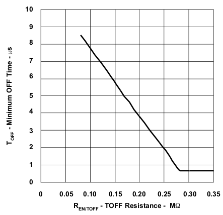
| REN/TOFF | EN/TOFF-to-GND resistor | 93 | 280 | kΩ | |
| tMIN | SYNC minimum pulse width at VTHSYNC – 0.1 V | 20 | ns | ||
6.4 Thermal Information
| THERMAL METRIC(1) | UCC24610 | UNIT | ||
|---|---|---|---|---|
| DRB (SON) | D (SOIC) | |||
| 9 PINS | 8 PINS | |||
| RθJA | Junction-to-ambient thermal resistance | 48.3 | 115.8 | °C/W |
| RθJC(top) | Junction-to-case (top) thermal resistance | 53.7 | 59.5 | °C/W |
| RθJB | Junction-to-board thermal resistance | 23.5 | 54.3 | °C/W |
| ψJT | Junction-to-top characterization parameter | 1.2 | 13.1 | °C/W |
| ψJB | Junction-to-board characterization parameter | 23.7 | 53.8 | °C/W |
| RθJC(bot) | Junction-to-case (bottom) thermal resistance | 8.1 | N/A | °C/W |
(1) For more information about traditional and new thermal metrics, see the the Semiconductor and IC Package Thermal Metrics application report, SPRA953.
6.5 Electrical Characteristics
At VCC = 5 VDC, CGATE = 0 pF, RTON = 200 kΩ, REN/TOFF = 100 kΩ, −40°C ≤ TJ = TA ≤ +125°C, all voltages are with respect to GND, and currents are positive into and negative out of the specified terminal, unless otherwise noted. Typical values are at TJ = +25°C.| PARAMETER | TEST CONDITIONS | MIN | TYP | MAX | UNIT | |
|---|---|---|---|---|---|---|
| BIAS SUPPLY | ||||||
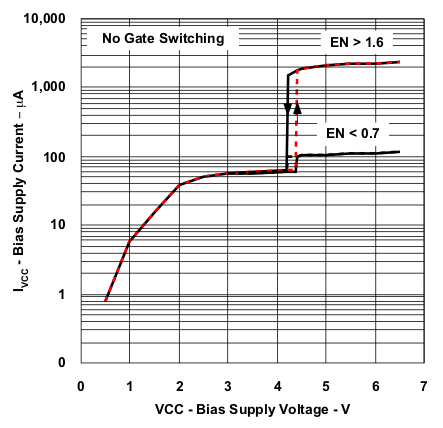
| ICCSTART | VCC current, undervoltage | VCC = 4.05 V | 70 | 100 | μA | |
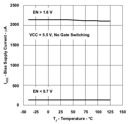
| ICCSTBY | VCC current, disabled | VCC = 5.5 V, REN/TOFF = 0 Ω | 130 | 200 | μA | |
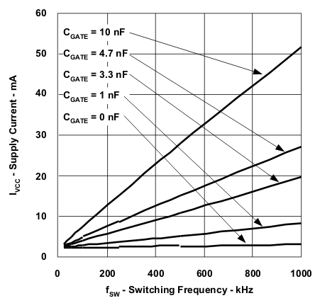
| ICCON | VCC current, enabled | VCC = 5.5 V, REN/TOFF = 100 kΩ | 1.40 | 2.15 | 2.80 | mA |
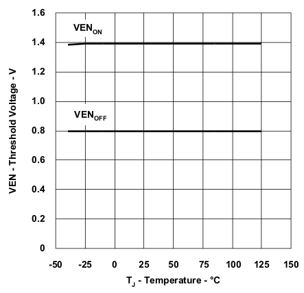
| VENON | EN/TOFF turnon threshold, rising | EN/TOFF driven, ICC > 1 mA | 1.31 | 1.40 | 1.49 | V |
| VENOFF | EN/TOFF turnoff threshold, falling | EN/TOFF driven, ICC < 200 µA | 0.74 | 0.80 | 0.86 | V |
| IEN-START | EN/TOFF input current, disabled | EN/TOFF = 1.3 V, rising from zero | –21.5 | –20.0 | –18.5 | μA |
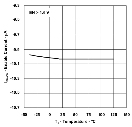
| IEN-ON | EN/TOFF input current, enabled | EN/TOFF = 2 V | –10.7 | –10.0 | –9.3 | μA |
| UNDERVOLTAGE LOCKOUT (UVLO) | ||||||
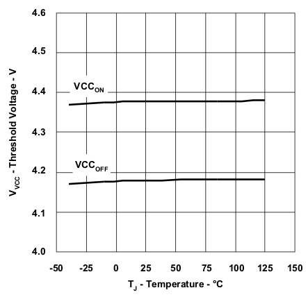
| VCCON | VCC turnon threshold | Turnon detected by VEN > 1.0 V | 4.15 | 4.40 | 4.65 | V |
| VCCOFF | VCC turnoff threshold | Turnoff detected by VEN < 0.5 V | 3.96 | 4.20 | 4.44 | V |
| VCCHYST | UVLO hysteresis | VCCHYST = VCCON – VCCOFF | 0.15 | 0.20 | 0.25 | V |
| MOSFET VOLTAGE SENSING | ||||||
| VTHARM | GATE rearming threshold | VD to GND, rising | 1.3 | 1.5 | 1.7 | V |
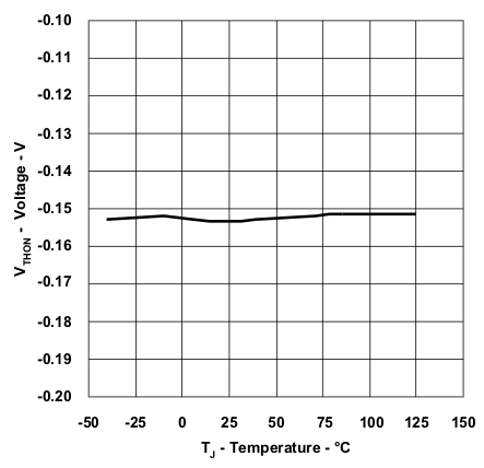
| VTHON | GATE turnon threshold | (VD – VS) falling, VS = 0 V | –220 | –150 | –80 | mV |
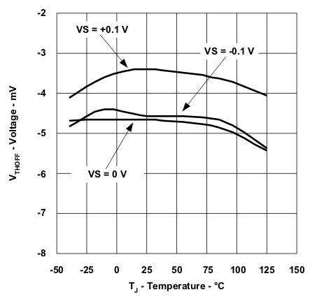
| VTHOFF | GATE turnoff threshold | (VD – VS) rising, VS = 0 V | –8 | –5 | –2 | mV |
| IDH | VD input bias current, high | VD = 50 V, VS = 0 V | 0.05 | 2.00 | μA | |
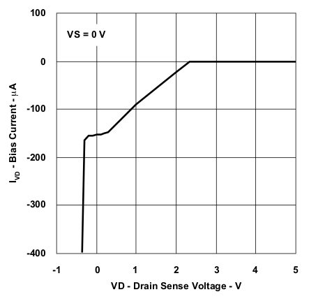
| IDL | VD input bias current, low | VD = -0.15 V, VS = 0 V | –250 | –150 | –50 | μA |
| IS | VS input bias current | VD = 0 V, VS = 0 V | –250 | –150 | –50 | μA |
| GATE DRIVER | ||||||
| rGUP | GATE pullup resistance, enabled | IGATE = –100 mA | 2.0 | 3.6 | Ω | |
| rGDN | GATE pulldown resistance, enabled | IGATE = 100 mA | 1.6 | 2.5 | Ω | |
| VOHG | GATE output high voltage | IGATE = –100 mA | 4.64 | 4.80 | V | |
| VOLG | GATE output low voltage | IGATE = 100 mA | 0.16 | 0.25 | V | |
| VOLGUV | GATE output low voltage, UV | IGATE = 25 mA, VCC = 0 V | 0.70 | 0.90 | V | |
| VOLGOFF | GATE output low voltage, disabled | IGATE = 25 mA, VEN = 0 V | 0.04 | 0.10 | V | |
| SYNCHRONIZATION | ||||||
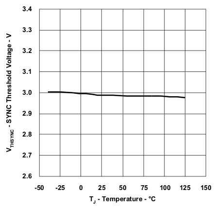
| VTHSYNC | SYNC falling threshold | GATE output transitions from high to low | VCC – 2.4 | VCC – 2.0 | VCC – 1.6 | V |
| rSYNC | SYNC pullup resistance | Internal resistance from SYNC to VCC | 1.6 | 2.0 | 2.4 | kΩ |
6.6 Timing Requirements
At VCC = 5 VDC, CGATE = 0 pF, RTON = 200 kΩ, REN/TOFF = 100 kΩ, −40°C ≤ TJ = TA ≤ +125°C, all voltages are with respect to GND, and currents are positive into and negative out of the specified terminal, unless otherwise noted. Typical values are at TJ = +25°C.| MIN | NOM | MAX | UNIT | ||
|---|---|---|---|---|---|
| MOSFET VOLTAGE SENSING | |||||
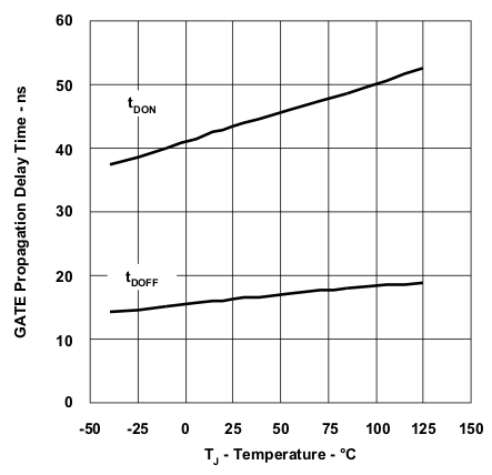
| tDON | GATE turnon propagation delay, from VTHON to GATE > 1 V | 44 | 70 | ns | |
| tDOFF | GATE turnoff propagation delay, from VTHOFF to GATE < 4 V | 16 | 35 | ns | |
| MINIMUM ON-TIME SETTING | |||||
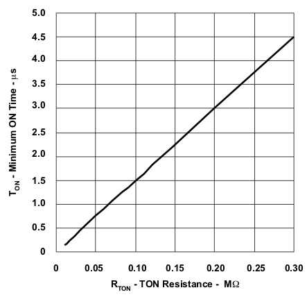
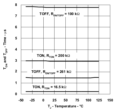
| tONLR | Minimum on-time, low resistance, RTON = 16.5 kΩ | 0.17 | 0.25 | 0.33 | μs |
| tONHR | Minimum on-time, high resistance, RTON = 200 kΩ | 2.2 | 3.0 | 3.8 | μs |
| MINIMUM OFF-TIME SETTING | |||||
| tOFFLR | Minimum off-time, low resistance, REN/TOFF = 100 kΩ | 4.94 | 7.80 | 9.86 | μs |
| tOFFHR | Minimum off-time, high resistance, REN/TOFF = 261 kΩ | 0.55 | 1.37 | 2.30 | μs |
| tOFFLV | Minimum off-time, low voltage, EN/TOFF = 1.0 V | 4.94 | 7.80 | 9.86 | μs |
| tOFFHV | Minimum off-time, high voltage, EN/TOFF = 2.61 V | 0.85 | 1.37 | 2.10 | μs |
| tOFFOV | Minimum off-time, over voltage, 3 V < VEN < VCC | 0.48 | 0.65 | 0.82 | μs |
| GATE DRIVER | |||||
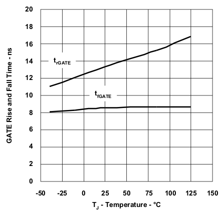
| tfGATE | GATE rise time, from 1 V to 4 V, CGATE = 3300 pF | 14 | 30 | ns | |
| trGATE | GATE fall time, from 4 V to 1 V, CGATE = 3300 pF | 9 | 25 | ns | |
| tDIS | Disable delay, from EN falling to GATE falling | 50 | 100 | 150 | ns |
| SYNCHRONIZATION | |||||
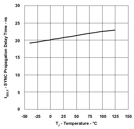
| tSDLY | SYNC propagation delay, from SYNC falling to GATE falling 10% | 20 | 60 | ns | |
6.7 Typical Characteristics
