SLUSC82A March 2015 – March 2015 UCC24630
PRODUCTION DATA.
- 1 Features
- 2 Applications
- 3 Description
- 4 Revision History
- 5 Pin Configuration and Functions
- 6 Specifications
- 7 Detailed Description
- 8 Application and Implementation
- 9 Power Supply Recommendations
- 10Layout
- 11Device and Documentation Support
- 12Mechanical, Packaging, and Orderable Information
- 13Mechanical, Packaging, and Orderable Information
Package Options
Mechanical Data (Package|Pins)
- DBV|6
Thermal pad, mechanical data (Package|Pins)
Orderable Information
8 Application and Implementation
NOTE
Information in the following applications sections is not part of the TI component specification, and TI does not warrant its accuracy or completeness. TI’s customers are responsible for determining suitability of components for their purposes. Customers should validate and test their design implementation to confirm system functionality.
8.1 Application Information
The UCC24630 is a high performance controller driver for N-channel MOSFET power devices used for secondary-side synchronous rectification. The UCC24630 is designed to operate as a companion device to a primary-side controller to help achieve efficient synchronous rectification in switching power supplies. The controller features a high-speed driver and provides appropriately timed logic circuitry that seamlessly generates an efficient synchronous rectification system. With its current emulator architecture, the UCC24630 has enough versatility to be applied in DCM, TM and CCM modes. The UCC24630 SR on-time adjustability allows optimizing for PSR and SSR applications. Additional features such as pin fault protection, dynamic VPC threshold sensing, and voltage sense blanking time and make the UCC24630 a robust synchronous controller. CCM dead-time protection shuts off the DRV signal in the event of an unstable switching frequency.
8.2 Typical Application
8.2.1 AC-to-DC Adapter, 19.5 V, 65 W
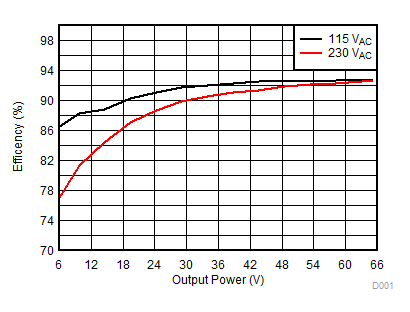
This design example describes the design of a 65-W off-line flyback converter providing 19.5 V at 3.33-A maximum load and operating from a universal AC input. The design uses the LM5023 AC-to-DC quasi-resonant primary-side controller in a DCM type flyback converter and achieves over 92% full-load efficiency with the use of the secondary side UCC24630 synchronous rectifier controller.
- The design requirements are detailed in Section 9.2.2
- The design procedure for selecting the component circuitry for use with the UCC24630 is detailed in Calculation of Component Values.
- Test results shown in section 9.2.4 highlight the unique advantages of using the UCC24630.
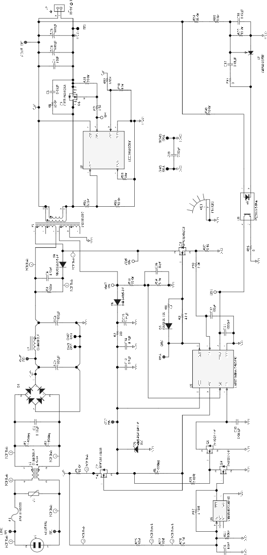 Figure 23. AC-to-DC Adapter 19 V, 65 W
8.2.2 Design Requirements
For this design example, use the parameters listed in Table 1.
Table 1. Performance Specifications AC-to-DC Adapter 19 V, 65 W
| PARAMETER | TEST CONDITIONS | MIN | NOM | MAX | UNIT | |
|---|---|---|---|---|---|---|
| Input Characteristics | ||||||
| VACIN | Input voltage | 90 | 115/230 | 265 | V | |
| fLINE | Frequency | 47 | 50/60 | 64 | Hz | |
| VAC(uvlo) | Brownout voltage | IOUT = IOUT(nom) | 80 | VRMS | ||
| VAC(run) | Brownout recovery voltage | 90 | VRMS | |||
| IIN | Input current | VACIN = VACIN(min), IOUT = IOUT(nom) | 1.65 | A | ||
| Output Characteristics | ||||||
| VOUT | Output voltage | VACIN = VACIN(min) to VACIN(max), IOUT = 0 to IOUT(nom) |
18.5 | 19.5 | 20.5 | V |
| IOUT(nom) | Nominal output current | VACIN = VACIN(min) to VACIN(max) | 3.33 | A | ||
| IOUT(min) | Minimum output current | VACIN = VACIN(min) to VACIN(max) | 0 | A | ||
| ΔVOUT | Output voltage ripple | VACIN = VACIN(min) to VACIN(max), IOUT = 0 to IOUT(nom) |
500 | mV | ||
| POUT | Output power | VACIN = VACIN(min) to VACIN(max) | 65 | |||
| System Characteristics | ||||||
| ηavg | Average efficiency | VACIN = VACIN(nom), IOUT = 25%, 50%, 75%, 100% of IOUT(nom) | 89% | 90% | ||
| ƞ10% | 10% Load efficiency | VACIN = VACIN(nom), IOUT = 10% of IOUT(nom) | 79% | 82% | ||
| PNL | No load power | VACIN = VACIN(nom), IOUT = 0 | 60 | 120 | mW | |
8.2.3 Calculation of Component Values
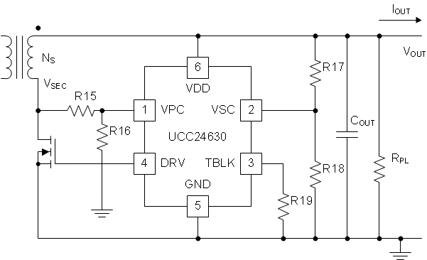 Figure 24. UCC24630 Circuit Design
For ease of understanding, Figure 24 is a modified version of Figure 17 where the component reference designators are the same as the schematic drawing of Figure 23.
8.2.3.1 VPC Input
For minimal power dissipation:
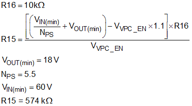
With R15 = 576 kΩ


Therefore, VVPC is within the recommended range of 0.45 V to 2 V.
8.2.3.2 VSC Input
The value of R18 is recommended to be with the range of 25 kΩ to 50 kΩ.
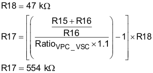
With R17 = 590 kΩ the operating range of the VSC pin is:


Therefore, VVSC is within the recommended range of 0.3 V to 2 V.
8.2.3.3 TBLK Input
The blanking time is set with resistor R19.
Select the blanking time to meet the following criteria based on minimum primary on-time at high line.
tVPC-BLK = (tPRI × 0.85) – 120 ns
spacer

A value of R19 = 18 kΩ results in a blanking time of approximately 420 ns.
8.2.4 Application Curves
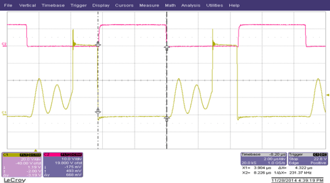
| C2(RED): DRV signal to synchronous rectifier Q1 | ||
| C1(YELLOW): Drain of synchronous rectifier Q1 |
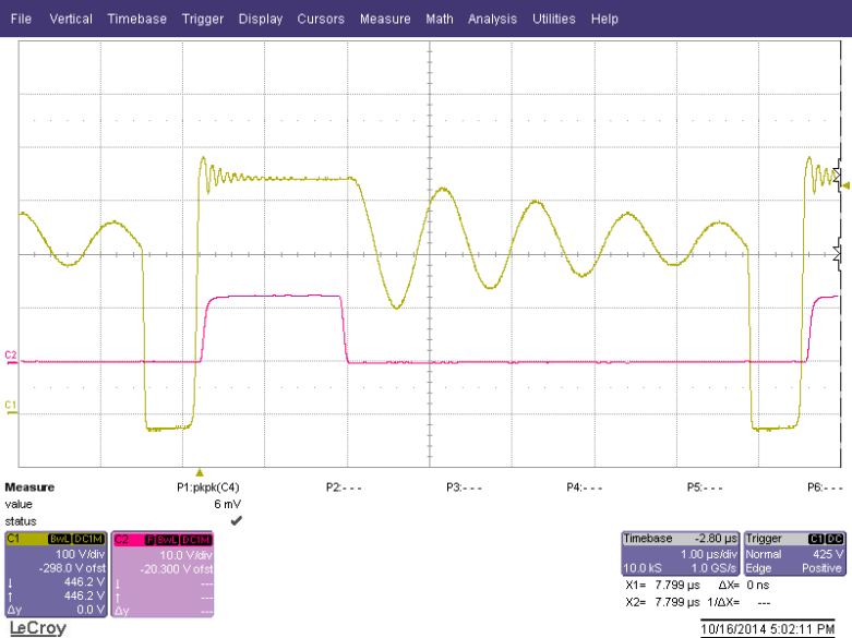
| C2(RED): DRV signal to synchronous rectifier Q1 | ||
| C1(YELLOW): Drain of primary-side MOSFET Q3 |

| C2(RED): DRV signal to synchronous rectifier Q1 | ||
| C1(YELLOW): Drain of synchronous rectifier Q1 |
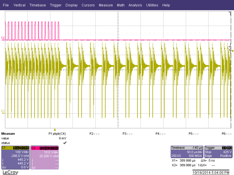
| C2(RED): DRV signal to synchronous rectifier Q1 | ||
| C1(YELLOW): Drain of primary-side MOSFET Q3 |
8.3 Do's and Don'ts
- Do operate the device within the recommended operating maximum parameters. Consider output overvoltage conditions when determining stress.
- Do consider the guideline for setting the blanking time resistor value illustrated in Figure 18.
- Do not use the UCC24630 with converters that operate in constant skip cycle mode at high-power levels. The skip cycle behavior results in numerous CCM faults and missing DRV pulses.
- Do not use the UCC24630 in CCM designs that are operating in CCM while the flyback controller is operating in variable frequency, FM, modulation. The CCM dead-time function is compatible with CCM operation during fixed-frequency, PWM operation.
- Do not use the UCC24630 in hysteretic control CCM flyback converters. Constant skip-cycle operation at high-power levels results in numerous CCM cycle faults resulting in efficiency loss.
- Do not use the UCC24630 in LLC converters.