SLUSCU6C August 2017 – January 2020 UCC256301
PRODUCTION DATA.
- 1 Features
- 2 Applications
- 3 Description
- 4 Revision History
- 5 Pin Configuration and Functions
- 6 Specifications
-
7 Detailed Description
- 7.1 Overview
- 7.2 Functional Block Diagram
- 7.3
Feature Description
- 7.3.1 Hybrid Hysteretic Control
- 7.3.2 Regulated 12-V Supply
- 7.3.3 Feedback Chain
- 7.3.4 Optocoupler Feedback Signal Input and Bias
- 7.3.5 System External Shut Down
- 7.3.6 Pick Lower Block and Soft Start Multiplexer
- 7.3.7 Pick Higher Block and Burst Mode Multiplexer
- 7.3.8 VCR Comparators
- 7.3.9 Resonant Capacitor Voltage Sensing
- 7.3.10 Resonant Current Sensing
- 7.3.11 Bulk Voltage Sensing
- 7.3.12 Output Voltage Sensing
- 7.3.13 High Voltage Gate Driver
- 7.3.14 Protections
- 7.4 Device Functional Modes
-
8 Application and Implementation
- 8.1 Application Information
- 8.2
Typical Application
- 8.2.1 Design Requirements
- 8.2.2
Detailed Design Procedure
- 8.2.2.1 LLC Power Stage Requirements
- 8.2.2.2 LLC Gain Range
- 8.2.2.3 Select Ln and Qe
- 8.2.2.4 Determine Equivalent Load Resistance
- 8.2.2.5 Determine Component Parameters for LLC Resonant Circuit
- 8.2.2.6 LLC Primary-Side Currents
- 8.2.2.7 LLC Secondary-Side Currents
- 8.2.2.8 LLC Transformer
- 8.2.2.9 LLC Resonant Inductor
- 8.2.2.10 LLC Resonant Capacitor
- 8.2.2.11 LLC Primary-Side MOSFETs
- 8.2.2.12 Design Considerations for Adaptive Dead-Time
- 8.2.2.13 LLC Rectifier Diodes
- 8.2.2.14 LLC Output Capacitors
- 8.2.2.15 HV Pin Series Resistors
- 8.2.2.16 BLK Pin Voltage Divider
- 8.2.2.17 BW Pin Voltage Divider
- 8.2.2.18 ISNS Pin Differentiator
- 8.2.2.19 VCR Pin Capacitor Divider
- 8.2.2.20 Burst Mode Programming
- 8.2.2.21 Soft-Start Capacitor
- 8.2.3 Application Curves
- 9 Power Supply Recommendations
- 10Layout
- 11Device and Documentation Support
- 12Mechanical, Packaging, and Orderable Information
Package Options
Mechanical Data (Package|Pins)
- DDB|14
Thermal pad, mechanical data (Package|Pins)
Orderable Information
8.2.2.20 Burst Mode Programming
The burst mode programming interface enables user to program a burst mode threshold voltage (VLL) which adaptively changes with input voltage. This way, consistent burst threshold can be achieved across VIN range, thus making the efficiency curve more consistent across VIN range.
The following relationship exists between VLL voltage and BLK pin voltage:

In this equation, VLL is the burst mode threshold voltage; VBLK is BLK pin voltage; two parameters a and b can be programmed by two external resistors.
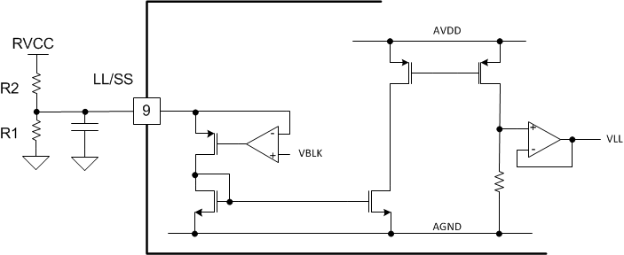
After soft start is done, the sensed BLK pin voltage is applied to LL/SS pin from inside the IC through a buffer. As shown in the figure below, this creates a difference between the current flowing through the programming resistor RLLUpper and RLLLower. The difference between the current flows into the LL/SS pin, mirrored and then applied to a 250-kΩ resistor RLL. The voltage on RLL is used as VLL.
 Figure 55. Burst Mode Programming
 The relationship between VLL and VBLK can then be derived:

Equation 69 rearranged produces Equation 70

To determine RLLUpper and RLLLower, two sets of (VLL, VBLK) values are required. VBLK can be measured directly from BLK pin. VLL level can be measured by inserting a 10-kΩ resistor between the feedback optocoupler emitter and ground. Assume the voltage measured on the 10-kΩ resistor is V10k. Then VLL voltage can be calculated as:

Remove the RLLUpper. In this way, the VLL voltage is at its minimal value 0.7 V, which is determined by the internal circuit design. Then adjust the load current to the desired burst mode threshold load level, and make sure the power stage does not burst in this condition. For example, 10% load is the desired burst mode threshold level. With 10 A as the full-load condition, set the load current to 1 A. After the load current is set, change the input voltage to two different voltages and record two different readings (V10k, VBLK). Then based on Equation 70 and Equation 71, RLLUpper and RLLLower can be solved.
In this example select the lower resistor to be 402 kΩ and the upper resistor to be 732 kΩ.