SLUSCU6C August 2017 – January 2020 UCC256301
PRODUCTION DATA.
- 1 Features
- 2 Applications
- 3 Description
- 4 Revision History
- 5 Pin Configuration and Functions
- 6 Specifications
-
7 Detailed Description
- 7.1 Overview
- 7.2 Functional Block Diagram
- 7.3
Feature Description
- 7.3.1 Hybrid Hysteretic Control
- 7.3.2 Regulated 12-V Supply
- 7.3.3 Feedback Chain
- 7.3.4 Optocoupler Feedback Signal Input and Bias
- 7.3.5 System External Shut Down
- 7.3.6 Pick Lower Block and Soft Start Multiplexer
- 7.3.7 Pick Higher Block and Burst Mode Multiplexer
- 7.3.8 VCR Comparators
- 7.3.9 Resonant Capacitor Voltage Sensing
- 7.3.10 Resonant Current Sensing
- 7.3.11 Bulk Voltage Sensing
- 7.3.12 Output Voltage Sensing
- 7.3.13 High Voltage Gate Driver
- 7.3.14 Protections
- 7.4 Device Functional Modes
-
8 Application and Implementation
- 8.1 Application Information
- 8.2
Typical Application
- 8.2.1 Design Requirements
- 8.2.2
Detailed Design Procedure
- 8.2.2.1 LLC Power Stage Requirements
- 8.2.2.2 LLC Gain Range
- 8.2.2.3 Select Ln and Qe
- 8.2.2.4 Determine Equivalent Load Resistance
- 8.2.2.5 Determine Component Parameters for LLC Resonant Circuit
- 8.2.2.6 LLC Primary-Side Currents
- 8.2.2.7 LLC Secondary-Side Currents
- 8.2.2.8 LLC Transformer
- 8.2.2.9 LLC Resonant Inductor
- 8.2.2.10 LLC Resonant Capacitor
- 8.2.2.11 LLC Primary-Side MOSFETs
- 8.2.2.12 Design Considerations for Adaptive Dead-Time
- 8.2.2.13 LLC Rectifier Diodes
- 8.2.2.14 LLC Output Capacitors
- 8.2.2.15 HV Pin Series Resistors
- 8.2.2.16 BLK Pin Voltage Divider
- 8.2.2.17 BW Pin Voltage Divider
- 8.2.2.18 ISNS Pin Differentiator
- 8.2.2.19 VCR Pin Capacitor Divider
- 8.2.2.20 Burst Mode Programming
- 8.2.2.21 Soft-Start Capacitor
- 8.2.3 Application Curves
- 9 Power Supply Recommendations
- 10Layout
- 11Device and Documentation Support
- 12Mechanical, Packaging, and Orderable Information
Package Options
Mechanical Data (Package|Pins)
- DDB|14
Thermal pad, mechanical data (Package|Pins)
Orderable Information
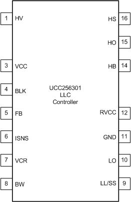
5 Pin Configuration and Functions
DDB Package
16-Pin SOIC
Top View

Pin Functions
| PIN | I/O | DESCRIPTION | |
|---|---|---|---|
| NAME | NO. | ||
| BLK | 4 | I | This pin is used to sense the PFC output voltage level. A resistive divider should be used to attenuate the signal before it is applied to this pin. The voltage level on this pin will determine when the LLC converter start/stops switching. The sensed BLK voltage is also used to adjust the burst mode threshold to improve efficiency over the input voltage range. |
| BW | 8 | I | This pin is used to sense the output voltage through the bias winding. The sensed voltage is used for output over voltage protection. |
| FB | 5 | I | LLC stage control feedback input. The amount of current sourced from this pin will determine the LLC input power level. |
| GND | 11 | G | Ground reference for all signals. |
| HB | 14 | I | High-side gate-drive floating supply voltage. The bootstrap capacitor is connected between this pin and pin HS. A high voltage, high speed diode should be connected from RVCC to this pin to supply power to the upper MOSFET driver during the period when the lower MOSFET is conducting. |
| HO | 15 | O | High-side floating gate-drive output. |
| HS | 16 | I | High-side gate-drive floating ground. Current return for the high-side gate-drive current. |
| HV | 1 | I | Connects to Internal HV startup JFET. This pin provides start up power for both PFC and LLC stage. This pin also monitors the AC line voltage for x-capacitor discharge function. |
| ISNS | 6 | I | Resonant current sense. The resonant capacitor voltage is differentiated with a first order filter to measure the resonant current |
| LL/SS | 9 | I | The capacitance value connected from this pin to ground will define the duration of the soft-start period. This pin is also used to program the burst mode threshold; the resistor divider on this pin programs the burst mode threshold and the threshold scaling factor with BLK pin voltage. |
| LO | 10 | O | Low-side gate-drive output. |
| Missing | 2 | N/A | Functional creepage and clearance |
| Missing | 13 | N/A | Functional creepage and clearance |
| RVCC | 12 | P | Regulated 12-V supply. This pin is used to supply the gate driver and PFC controller. |
| VCC | 3 | P | Supply input. |
| VCR | 7 | I | Resonant capacitor voltage sense |