SLUSAY4D March 2012 – December 2014 UCC27516 , UCC27517
PRODUCTION DATA.
- 1 Features
- 2 Applications
- 3 Description
- 4 Revision History
- 5 Description (continued)
- 6 Device Comparison Table
- 7 Pin Configuration and Functions
- 8 Specifications
- 9 Detailed Description
- 10Application and Implementation
- 11Power Supply Recommendations
- 12Layout
- 13Device and Documentation Support
- 14Mechanical, Packaging, and Orderable Information
Package Options
Mechanical Data (Package|Pins)
- DBV|5
Thermal pad, mechanical data (Package|Pins)
Orderable Information
8 Specifications
8.1 Absolute Maximum Ratings(1)(2)(3)
over operating free-air temperature range (unless otherwise noted)| MIN | MAX | UNIT | |||
|---|---|---|---|---|---|
| Supply voltage | VDD | –0.3 | 20 | V | |
| OUT voltage | DC | –0.3 | VDD + 0.3 | ||
| Repetitive pulse less than 200 ns(5) | –2 | VDD + 0.3 | |||
| Output continuous current | IOUT_DC (source/sink) | 0.3 | A | ||
| Output pulsed current (0.5 µs) | IOUT_pulsed(source/sink) | 4 | |||
| IN+, IN-(4) | –0.3 | 20 | V | ||
| Operating virtual junction temperature, TJ | –40 | 150 | °C | ||
| Lead temperature | Soldering, 10 sec. | 300 | |||
| Reflow | 260 | ||||
| Storage temperature, Tstg | –65 | 150 | |||
(1) Stresses beyond those listed under Absolute Maximum Ratings may cause permanent damage to the device. These are stress ratings only and functional operation of the device at these or any other conditions beyond those indicated under Recommended Operating Conditions is not implied. Exposure to absolute-maximum-rated conditions for extended periods may affect device reliability.
(2) All voltages are with respect to GND unless otherwise noted. Currents are positive into, negative out of the specified terminal. See Packaging Section of the datasheet for thermal limitations and considerations of packages.
(3) These devices are sensitive to electrostatic discharge; follow proper device-handling procedures.
(4) Maximum voltage on input pins is not restricted by the voltage on the VDD pin.
8.2 ESD Ratings
| VALUE | UNIT | |||
|---|---|---|---|---|
| V(ESD) | Electrostatic discharge | Human body model (HBM), per ANSI/ESDA/JEDEC JS-001(1) | ±4000 | V |
| Charged-device model (CDM), per JEDEC specification JESD22-C101(2) | ±1000 | |||
(1) JEDEC document JEP155 states that 500-V HBM allows safe manufacturing with a standard ESD control process.
(2) JEDEC document JEP157 states that 250-V CDM allows safe manufacturing with a standard ESD control process.
8.3 Recommended Operating Conditions
over operating free-air temperature range (unless otherwise noted)| MIN | NOM | MAX | UNIT | |
|---|---|---|---|---|
| Supply voltage range, VDD | 4.5 | 12 | 18 | V |
| Operating junction temperature range | –40 | 140 | °C | |
| Input voltage, IN+ and IN- | 0 | 18 | V |
8.4 Thermal Information
| THERMAL METRIC(1) | UCC27516 | UCC27517 | UNIT | |
|---|---|---|---|---|
| WSON | SOT-23 | |||
| 6 PINS | 5 PINS | |||
| RθJA | Junction-to-ambient thermal resistance | 85.6 | 217.6 | °C/W |
| RθJC(top) | Junction-to-case (top) thermal resistance | 100.1 | 85.8 | |
| RθJB | Junction-to-board thermal resistance | 58.6 | 44.0 | |
| ψJT | Junction-to-top characterization parameter | 7.5 | 4.0 | |
| ψJB | Junction-to-board characterization parameter | 58.7 | 43.2 | |
| RθJC(bot) | Junction-to-case (bottom) thermal resistance | 23.7 | n/a | |
(1) For more information about traditional and new thermal metrics, see the IC Package Thermal Metrics application report, SPRA953.
8.5 Electrical Characteristics
VDD = 12 V, TA = TJ = –40°C to 140°C, 1-µF capacitor from VDD to GND. Currents are positive into, negative out of the specified pin.| PARAMETER | TEST CONDITIONS | MIN | TYP | MAX | UNIT | ||
|---|---|---|---|---|---|---|---|
| BIAS CURRENTS | |||||||
| IDD(off) | Startup current | VDD = 3.4 V | IN+ = VDD, IN- = GND | 40 | 100 | 160 | µA |
| IN+ = IN- = GND or IN+ = IN- = VDD | 25 | 75 | 145 | ||||
| IN+ = GND, IN- = VDD | 20 | 60 | 115 | ||||
| UNDERVOLTAGE LOCKOUT (UVLO) | |||||||
| VON | Supply start threshold | TA = 25°C | 3.91 | 4.20 | 4.5 | V | |
| TA = –40°C to 140°C | 3.70 | 4.20 | 4.65 | ||||
| VOFF | Minimum operating voltage after supply start | 3.45 | 3.9 | 4.35 | |||
| VDD_H | Supply voltage hysteresis | 0.2 | 0.3 | 0.5 | |||
| INPUTS (IN+, IN-) | |||||||
| VIN_H | Input signal high threshold | Output high for IN+ pin, Output low for IN- pin |
2.2 | 2.4 | V | ||
| VIN_L | Input signal low threshold | Output low for IN+ pin, Output high for IN- pin |
1.0 | 1.2 | |||
| VIN_HYS | Input signal hysteresis | 1.0 | |||||
| SOURCE/SINK CURRENT | |||||||
| ISRC/SNK | Source/sink peak current(1) | CLOAD = 0.22 µF, FSW = 1 kHz | ±4 | A | |||
| OUTPUTS (OUT) | |||||||
| VDD-VOH | High output voltage | VDD = 12 V IOUT = –10 mA |
50 | 90 | mV | ||
| VDD = 4.5 V IOUT = –10 mA |
60 | 130 | |||||
| VOL | Low output voltage | VDD = 12 IOUT = 10 mA |
5 | 10 | |||
| VDD = 4.5 V IOUT = 10 mA |
6 | 12 | |||||
| ROH | Output pullup resistance(2) | VDD = 12 V IOUT = –10 mA |
5.0 | 7.5 | Ω | ||
| VDD = 4.5 V IOUT = –10 mA |
5.0 | 11.0 | |||||
| ROL | Output pulldown resistance | VDD = 12 V IOUT = 10 mA |
0.5 | 1.0 | |||
| VDD = 4.5 V IOUT = 10 mA |
0.6 | 1.2 | |||||
(1) Ensured by Design.
(2) ROH represents on-resistance of P-Channel MOSFET in pullup structure of the UCC27516 and UCC27517's output stage.
8.6 Switching Characteristics
over operating free-air temperature range (unless otherwise noted)| PARAMETER | TEST CONDITIONS | MIN | TYP | MAX | UNIT | |
|---|---|---|---|---|---|---|
| tR | Rise time(1) | VDD = 12 V CLOAD = 1.8 nF |
8 | 12 | ns | |
| VDD = 4.5 V CLOAD = 1.8 nF |
16 | 22 | ||||
| tF | Fall time(1) | VDD = 12 V CLOAD = 1.8 nF |
7 | 11 | ||
| VDD=4.5V CLOAD = 1.8 nF |
7 | 11 | ||||
| tD1 | IN+ to output propagation delay(1) | VDD = 12 V 5-V input pulse CLOAD = 1.8 nF |
4 | 13 | 23 | |
| VDD = 4.5 V 5-V input pulse CLOAD = 1.8 nF |
4 | 15 | 26 | |||
| tD2 | IN- to output propagation delay(1) | VDD = 12 V CLOAD = 1.8 nF |
4 | 13 | 23 | |
| VDD = 4.5 V CLOAD = 1.8 nF |
4 | 19 | 30 | |||
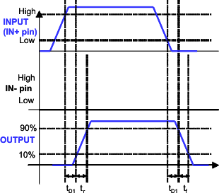
(PWM Input to IN+ Pin (IN– Pin Tied to GND))
Figure 1. Noninverting Configuration
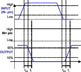
(PWM Input to IN- Pin (IN+ Pin Tied to VDD))
Figure 2. Inverting Configuration
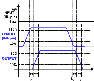
(Enable and Disable Signal Applied to IN+ Pin, PWM Input to IN- Pin)
Figure 3. Enable and Disable Function Using IN+ Pin
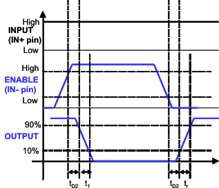
(Enable and Disable Signal Applied to IN- Pin, PWM Input to IN+ Pin)
Figure 4. Enable and Disable Function Using IN- Pin
8.7 Typical Characteristics
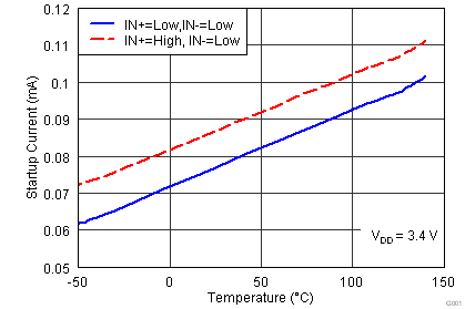 Figure 5. Startup Current vs Temperature
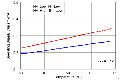 Figure 7. Supply Current vs Temperature (Output In DC On/Off Condition)
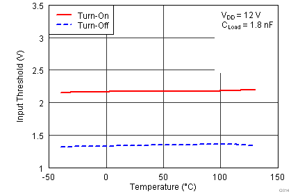 Figure 9. Input Threshold vs Temperature
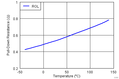 Figure 11. Output Pulldown Resistance vs Temperature
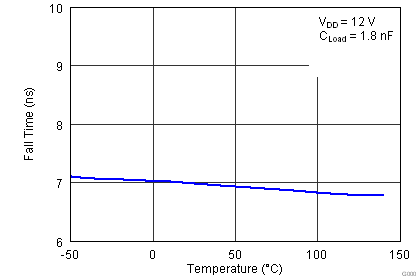 Figure 13. Fall Time vs Temperature
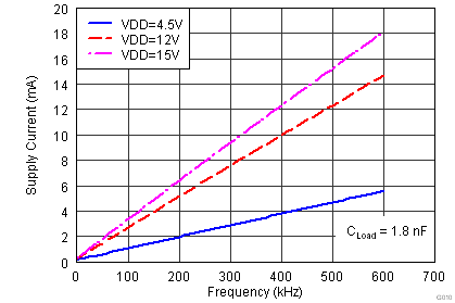 Figure 15. Operating Supply Current vs Frequency
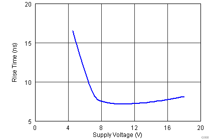 Figure 17. Rise Time vs Supply Voltage
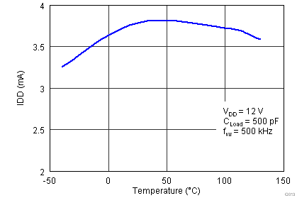 Figure 6. Operating Supply Current vs Temperature (Output Switching)
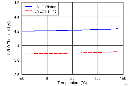 Figure 8. UVLO Threshold Voltage vs Temperature
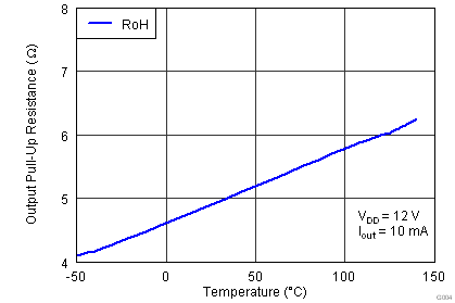 Figure 10. Output Pullup Resistance vs Temperature
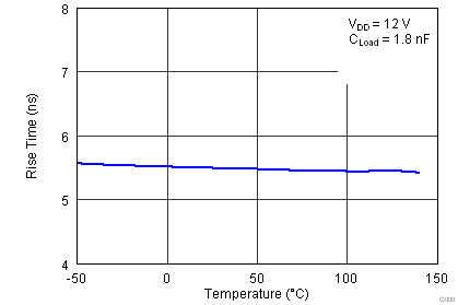 Figure 12. Rise Time vs Temperature
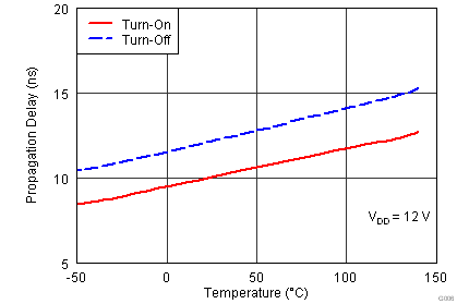 Figure 14. Input To Output Propagation Delay vs Temperature
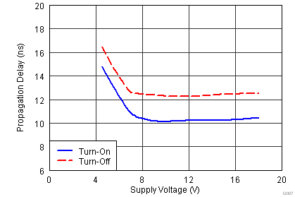 Figure 16. Propagation Delays vs Supply Voltage
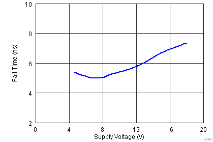 Figure 18. Fall Time vs Supply Voltage