SLUSB41A July 2012 – December 2014 UCC28700 , UCC28701 , UCC28702 , UCC28703
PRODUCTION DATA.
- 1 Features
- 2 Applications
- 3 Description
- 4 Revision History
- 5 Device Comparison Table
- 6 Pin Configuration and Functions
- 7 Specifications
- 8 Detailed Description
-
9 Applications and Implementation
- 9.1 Application Information
- 9.2
Typical Application
- 9.2.1 Design Requirements
- 9.2.2
Detailed Design Procedure
- 9.2.2.1 Transformer Parameter Verification
- 9.2.2.2 Output Capacitance
- 9.2.2.3 VDD Capacitance, CDD
- 9.2.2.4 VDD Start-Up Resistance, RSTR
- 9.2.2.5 VS Resistor Divider, Line Compensation, and Cable Compensation
- 9.2.2.6 Input Bulk Capacitance and Minimum Bulk Voltage
- 9.2.2.7 Transformer Turns Ratio, Inductance, Primary-Peak Current
- 9.2.2.8 Standby Power Estimate
- 9.2.3 Application Curves
- 10Power Supply Recommendations
- 11Layout
-
12Device and Documentation Support
- 12.1
Device Support
- 12.1.1
Device Nomenclature
- 12.1.1.1 Capacitance Terms in Farads
- 12.1.1.2 Duty Cycle Terms
- 12.1.1.3 Frequency Terms in Hertz
- 12.1.1.4 Current Terms in Amperes
- 12.1.1.5 Current and Voltage Scaling Terms
- 12.1.1.6 Transformer Terms
- 12.1.1.7 Power Terms in Watts
- 12.1.1.8 Resistance Terms in Ω
- 12.1.1.9 Timing Terms in Seconds
- 12.1.1.10 Voltage Terms in Volts
- 12.1.1.11 AC Voltage Terms in VRMS
- 12.1.1.12 Efficiency Terms
- 12.1.1
Device Nomenclature
- 12.2 Documentation Support
- 12.3 Trademarks
- 12.4 Electrostatic Discharge Caution
- 12.5 Glossary
- 12.1
Device Support
- 13Mechanical, Packaging, and Orderable Information
Package Options
Mechanical Data (Package|Pins)
- DBV|6
Thermal pad, mechanical data (Package|Pins)
Orderable Information
7 Specifications
7.1 Absolute Maximum Ratings(1)
over operating free-air temperature range (unless otherwise noted)| MIN | MAX | UNIT | ||
|---|---|---|---|---|
| Bias supply voltage | VVDD | 38 | V | |
| Continuous gate current sink | IDRV | 50 | mA | |
| Continuous gate current source | IDRV | Self-limiting | ||
| Peak VS pin current | IVS | −1.2 | ||
| Gate-drive voltage at DRV | VDRV | −0.5 | Self-limiting | V |
| Voltage range | VS | −0.75 | 7 | |
| CS, CBC (UCC28700), NTC (UCC28701/2/3) |
−0.5 | 5 | ||
| Operating junction temperature range | TJ | −55 | 150 | °C |
| Lead temperature 0.6 mm from case for 10 seconds | 260 | |||
| Storage temperature, Tstg | –65 | 150 | °C | |
(1) Stresses beyond those listed under Absolute Maximum Ratings may cause permanent damage to the device. These are stress ratings only and functional operation of the device at these or any other conditions beyond those indicated under Recommended Operating Conditions is not implied. Exposure to absolute-maximum-rated conditions for extended periods may affect device reliability. All voltages are with respect to GND. Currents are positive into, negative out of the specified terminal. These ratings apply over the operating ambient temperature ranges unless otherwise noted.
7.2 ESD Ratings
| VALUE | UNIT | |||
|---|---|---|---|---|
| V(ESD) | Electrostatic discharge | Human-body model (HBM), per ANSI/ESDA/JEDEC JS-001(1) | ±2000 | V |
| Charged-device model (CDM), per JEDEC specification JESD22-C101(2) | ±500 | |||
(1) JEDEC document JEP155 states that 500-V HBM allows safe manufacturing with a standard ESD control process.
(2) JEDEC document JEP157 states that 250-V CDM allows safe manufacturing with a standard ESD control process.
7.3 Recommended Operating Conditions
over operating free-air temperature range (unless otherwise noted)| MIN | MAX | UNIT | ||
|---|---|---|---|---|
| VDD | Bias supply operating voltage | 9 | 35 | V |
| CVDD | VDD bypass capacitor | 0.047 | 1 | µF |
| RCBC | Cable-compensation resistance | 10 | kΩ | |
| IVS | VS pin current | −1 | mA | |
| TJ | Operating junction temperature | −20 | 125 | °C |
7.4 Thermal Information
| THERMAL METRIC(1) | UCC2870x | UNIT | |
|---|---|---|---|
| DBV | |||
| 6 PINS | |||
| θJA | Junction-to-ambient thermal resistance(2) | 180 | °C/W |
| θJCtop | Junction-to-case (top) thermal resistance(3) | 71.2 | |
| θJB | Junction-to-board thermal resistance(4) | 44.4 | |
| ψJT | Junction-to-top characterization parameter(5) | 5.1 | |
| ψJB | Junction-to-board characterization parameter(6) | 43.8 | |
(1) For more information about traditional and new thermal metrics, see the IC Package Thermal Metrics application report, SPRA953.
(2) The junction-to-ambient thermal resistance under natural convection is obtained in a simulation on a JEDEC-standard, high-K board, as specified in JESD51-7, in an environment described in JESD51-2a.
(3) The junction-to-case (top) thermal resistance is obtained by simulating a cold plate test on the package top. No specific JEDEC-standard test exists, but a close description can be found in the ANSI SEMI standard G30-88.
(4) The junction-to-board thermal resistance is obtained by simulating in an environment with a ring cold plate fixture to control the PCB temperature, as described in JESD51-8.
(5) The junction-to-top characterization parameter, ψJT, estimates the junction temperature of a device in a real system and is extracted from the simulation data for obtaining RθJA, using a procedure described in JESD51-2a (sections 6 and 7).
(6) The junction-to-board characterization parameter, ψJB, estimates the junction temperature of a device in a real system and is extracted from the simulation data for obtaining RθJA, using a procedure described in JESD51-2a (sections 6 and 7).
7.5 Electrical Characteristics
over operating free-air temperature range, VDD = 25 V, RCBC = RNTC = open, –20°C ≤ TA ≤ 125°C, TJ = TA(unless otherwise noted)
| PARAMETER | TEST CONDITIONS | MIN | TYP | MAX | UNITS | |
|---|---|---|---|---|---|---|
| BIAS SUPPLY INPUT | ||||||
| IRUN | Supply current, run | IDRV = 0, run state | 2.1 | 2.65 | mA | |
| IWAIT | Supply current, wait | IDRV = 0, wait state | 85 | 110 | µA | |
| ISTART | Supply current, start | IDRV = 0, VVDD = 18 V, start state | 1 | 1.5 | ||
| IFAULT | Supply current, fault | IDRV = 0, fault state | 2.1 | 2.8 | mA | |
| UNDER-VOLTAGE LOCKOUT | ||||||
| VVDD(on) | VDD turn-on threshold | VVDD low to high | 19 | 21 | 23 | V |
| VVDD(off) | VDD turn-off threshold | VVDD high to low | 7.7 | 8.1 | 8.45 | |
| VS INPUT | ||||||
| VVSR | Regulating level | Measured at no-load condition, TJ = 25°C | 4.01 | 4.05 | 4.09 | V |
| VVSNC | Negative clamp level | IVS = -300 µA, volts below ground | 190 | 250 | 325 | mV |
| IVSB | Input bias current | VVS = 4 V | –0.25 | 0 | 0.25 | µA |
| CS INPUT | ||||||
| VCST(max) | Max CS threshold voltage | VVS = 3.7 V(1) | 715 | 750 | 775 | mV |
| VCST(min) | Min CS threshold voltage | VVS = 4.35 V(1) | 230 | 250 | 270 | |
| KAM | AM control ratio | VCST(max) / VCST(min) | 2.75 | 3.0 | 3.15 | V/V |
| VCCR | constant-current regulating level | CC regulation constant | 310 | 319 | 329 | mV |
| KLC | Line compensating current ratio | IVSLS = -300 µA, IVSLS / current out of CS pin | 23 | 25 | 28 | A/A |
| TCSLEB | Leading-edge blanking time | DRV output duration, VCS = 1 V | 195 | 235 | 275 | ns |
| DRV | ||||||
| IDRS | DRV source current | VDRV = 8 V, VVDD = 9 V | 20 | 25 | mA | |
| RDRVLS | DRV low-side drive resistance | IDRV = 10 mA | 6 | 12 | Ω | |
| VDRCL | DRV clamp voltage | VVDD = 35 V | 14 | 16 | V | |
| RDRVSS | DRV pull-down in start state | 150 | 200 | 230 | kΩ | |
| PROTECTION | ||||||
| VOVP | Over-voltage threshold | At VS input, TJ = 25°C | 4.52 | 4.6 | 4.68 | V |
| VOCP | Over-current threshold | At CS input | 1.4 | 1.5 | 1.6 | |
| IVSL(run) | VS line-sense run current | Current out of VS pin – increasing | 190 | 220 | 260 | µA |
| IVSL(stop) | VS line-sense stop current | Current out of VS pin – decreasing | 70 | 80 | 95 | |
| KVSL | VS line-sense ratio | IVSL(run) / IVSL(stop) | 2.5 | 2.8 | 3.05 | A/A |
| TJ(stop) | Thermal shut-down temperature | Internal junction temperature | 165 | °C | ||
| CABLE COMPENSATION (UCC28700 ONLY) | ||||||
| VCBC(max) | Cable compensation maximum voltage | Voltage at CBC at full load | 2.8 | 3.0 | 3.4 | V |
| VCVS(min) | Compensation at VS | VCBC = open, change in VS regulating level at full load | –45 | –15 | 25 | mV |
| VCVS(max) | Maximum compensation at VS | VCBC = 0 V, change in VS regulating level at full load | 275 | 320 | 365 | |
| CABLE COMPENSATION (UCC28701, UCC28702, AND UCC28703 ONLY) | ||||||
| VCVS | Compensation at VS (UCC28701) | Change in VS regulating level at full load | –45 | –15 | 25 | mV |
| VCVS | Compensation at VS (UCC28702) | Change in VS regulating level at full load | 100 | |||
| VCVS | Compensation at VS (UCC28703) | Change in VS regulating level at full load | 200 | |||
| NTC INPUT (UCC28701, UCC28702, AND UCC28703 ONLY) | ||||||
| VNTCTH | NTC shut-down threshold | Fault UVLO cycle when below this threshold | 0.95 | V | ||
| INTC | NTC pull-up current | Current out of pin | 105 | µA | ||
(1) These devices automatically vary the control frequency and current sense thresholds to improve EMI performance, these threshold voltages and frequency limits represent average levels.
7.6 Switching Characteristics
over operating free-air temperature range (unless otherwise noted)| PARAMETER | TEST CONDITIONS | MIN | TYP | MAX | UNIT | |
|---|---|---|---|---|---|---|
| fSW(max) | Maximum switching frequency | VVS = 3.7 V(1) | 120 | 130 | 140 | kHz |
| fSW(min) | Minimum switching frequency | VVS = 4.35 V(1) | 875 | 1000 | 1100 | Hz |
| TZTO | Zero-crossing timeout delay | 1.8 | 2.1 | 2.45 | µs | |
7.7 Typical Characteristics
At VDD = 25 V, unless otherwise noted.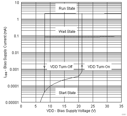 Figure 1. Bias Supply Current vs. Bias Supply Voltage
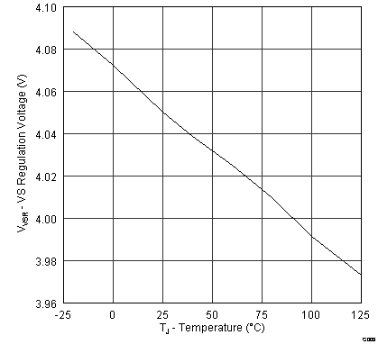 Figure 3. VS Regulation Voltage vs. Temperature
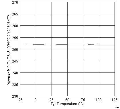 Figure 5. Minimum CS Threshold Voltage vs. Temperature
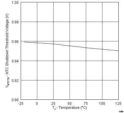 Figure 9. NTC Shutdown Threshold Voltage vs. Temperature
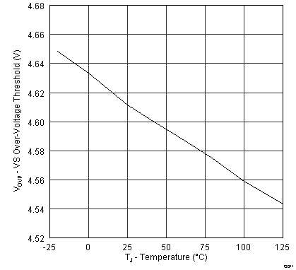 Figure 11. Overvoltage Threshold vs. Temperature
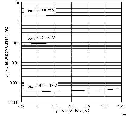 Figure 2. Bias Supply Current vs. Temperature
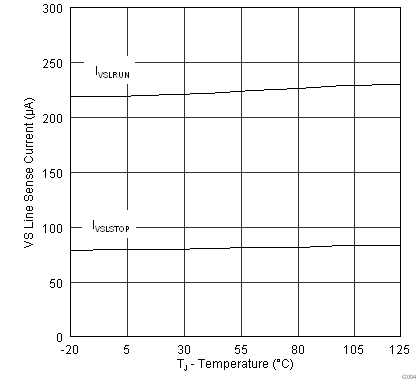 Figure 4. Line-Sense Current vs. Temperature
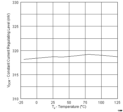 Figure 6. Constant-Current Regulating Level vs. Temperature
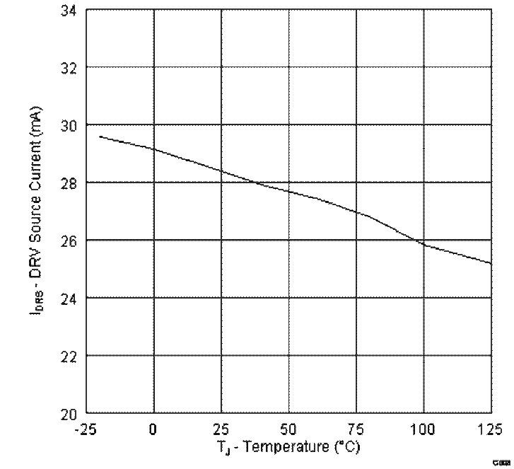
| VDRV = 8 V, VVDD = 9 V |
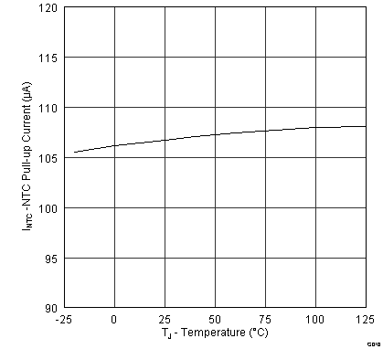 Figure 10. NTC Pullup Current vs. Temperature