SLUSBL5A February 2015 – June 2019 UCC28730
PRODUCTION DATA.
- 1 Features
- 2 Applications
- 3 Description
- 4 Revision History
- 5 Pin Configuration and Functions
- 6 Specifications
-
7 Detailed Description
- 7.1 Overview
- 7.2 Functional Block Diagram
- 7.3 Feature Description
- 7.4 Device Functional Modes
-
8 Application and Implementation
- 8.1 Application Information
- 8.2
Typical Application
- 8.2.1 Design Requirements
- 8.2.2
Detailed Design Procedure
- 8.2.2.1 Stand-By Power Estimate
- 8.2.2.2 Input Bulk Capacitance and Minimum Bulk Voltage
- 8.2.2.3 Transformer Turns Ratio, Inductance, Primary-Peak Current
- 8.2.2.4 Transformer Parameter Verification
- 8.2.2.5 Output Capacitance
- 8.2.2.6 VDD Capacitance, CVDD
- 8.2.2.7 VS Resistor Divider, Line Compensation, and Cable Compensation
- 8.2.2.8 VS Wake-Up Detection
- 8.2.3 Application Curves
- 8.3 Do's and Don'ts
- 9 Power Supply Recommendations
- 10Layout
-
11Device and Documentation Support
- 11.1
Device Support
- 11.1.1 Development Support
- 11.1.2
Device Nomenclature
- 11.1.2.1 Capacitance Terms in Farads
- 11.1.2.2 Duty-Cycle Terms
- 11.1.2.3 Frequency Terms in Hertz
- 11.1.2.4 Current Terms in Amperes
- 11.1.2.5 Current and Voltage Scaling Terms
- 11.1.2.6 Transformer Terms
- 11.1.2.7 Power Terms in Watts
- 11.1.2.8 Resistance Terms in Ω
- 11.1.2.9 Timing Terms in Seconds
- 11.1.2.10 DC Voltage Terms in Volts
- 11.1.2.11 AC Voltage Terms in Volts
- 11.1.2.12 Efficiency Terms
- 11.2 Documentation Support
- 11.3 Receiving Notification of Documentation Updates
- 11.4 Community Resources
- 11.5 Trademarks
- 11.6 Electrostatic Discharge Caution
- 11.7 Glossary
- 11.1
Device Support
- 12Mechanical, Packaging, and Orderable Information
Package Options
Mechanical Data (Package|Pins)
- D|7
Thermal pad, mechanical data (Package|Pins)
Orderable Information
7.3.6 Valley-Switching and Valley-Skipping
The UCC28730 utilizes valley-switching to reduce switching losses in the MOSFET, to reduce induced-EMI, and to minimize the turn-on current spike at the current-sense resistor. The controller operates in valley-switching in all load conditions unless the VDS ringing is diminished to the point where valleys are no longer detectable.
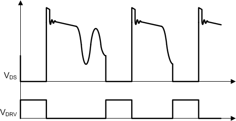
As shown in Figure 22, the UCC28730 operates in a valley-skipping mode (also known as valley-hopping) in most load conditions to maintain an accurate voltage or current regulation point and still switch on the lowest available VDS voltage.
 Figure 22. Valley-Skipping Mode
 Valley-skipping modulates each switching cycle into discrete period durations. During FM operation, the switching cycles are periods when energy is delivered to the output in fixed packets, and the power delivered varies inversely with the switching period. During operating conditions when the switching period is relatively short, such as at high-load and low-line, the average power delivered per cycle varies significantly based on the number of valleys skipped between cycles. As a consequence, valley-skipping adds additional low-amplitude ripple voltage to the output with a frequency dependent upon the rate of change of the bulk voltage. For a load with an average power level between that of cycles with fewer valleys skipped and cycles with more valleys skipped, the voltage-control loop modulates the control law voltage and toggles between longer and shorter switching periods to match the required average output power.